Tahoma Technology
Model 10116/10118
High Performance
DR11-W Emulator
for PCI Bus
5 September, 2008
Contents
Introduction to Detailed Specifications
Device Interface - timing (non-burst mode)
Device Interface - timing (burst mode output)
Model 10116/10118
PCI DR11-W Emulator
Tahoma Technology
2819 Elliott Avenue, Suite 206
Seattle, WA, USA, 98121
phone: 206.728.6465
fax: 206.728.1633
This document describes Tahoma Technology’s Models 10116 and 10118 PCI DR11-W emulators. Included are basic hardware and software installation instructions, as well as detailed technical information appropriate to the device driver programmer.
The 10116 and 10118 are high-performance PCI boards capable of connecting to any device or system which supports the DEC DR11-W interface specification. Tahoma Technology’s DR11-W compatible interfaces may be used for very high speed 16-bit parallel connections to external devices, or back-to-back with other DR11-W interfaces in interprocessor links. The 10116 is a full size PCI card that provides DEC compatible 40-pin header style connectors, as well as an 80-pin high density connector. The 10118 is a ½ size PCI board that provides only the 80 pin connector.
Both boards are PCI bus-master capable with 16K bytes of on-board FIFO buffer memory (8K each for input and output). Scatter/gather DMA and burst transfers can transfer data to and from the attached at up to 8Mbyes/second (20Mbytes/second output in Tahoma Burst Mode).
Multiple operating modes, programmable handshake speeds and protocols, and a variety of cabling options provide flexibility to support a wide range of devices and host systems.
Tahoma - The Chinook jargon name for Mt. Rainier
Tahoma Technology is a new company with a 40+ year history.
The original Ikon Corporation was founded in 1966. In its early years, Ikon Corporation designed and built minicomputer based systems and specialized peripheral equipment. With the advent of personal work stations, Ikon Corporation found a market for high performance interface products - initially for the Multibus. The first product was a Multibus based Versatec (VPI) interface for electrostatic plotters, followed by a DR11-W emulator which allowed supporting VAX related external hardware and interprocessor links on Apollo work stations. VPI was adopted by many printer and plotter manufacturers as the interface of choice. The DR11 became a standard for high-speed 16 bit interfacing. As new bus architectures came on line, these interfaces were ported to new host busses, including, among others, VersaBus, VMEbus, ISA, EISA, MicroChannel, Sbus, and PCI. Along with the bus migration, Centronics compatibility was added to the plotter interfaces, and speeds continued to improve. Today, the PCI plotter interface bursts data from the bus at 40MB/sec, and feeds the plotter at 4-5MB/sec. The PCI DR11-W can sustain 20MB/sec outputs.
In 1997, Ikon Corporation was acquired by IKON Office Solutions (IOS) and became the Ikon Corporation division of IOS.
In August, 2001, the people from the original Ikon Corporation, who had continued to run Ikon Corporation as an IOS division, formed Tahoma Technology and purchased certain of the assets of Ikon Corporation. It has been an enjoyable four years with the IOS, but we are happy and excited to be back on our own.
Tahoma Technology has acquired certain of the assets and liabilities of Ikon Corporation, including warranty support. While the asset purchase was definitely NOT a name change (Tahoma Technology is a new entity; the Ikon Corporation name, marks, and structure remain with IOS), the impact on our customer base should be nil, beyond changing the name in the address book. We are the same people, with the same high performance products, and the same attitude about customer support. We look forward to continuing our 35 year relationship with our customers under the new banner.
In 2002, Tahoma Technology added the 10119, 10120, and 10121 family of IEEE1284 and Ethernet to VPI converters to the product line.
Please note that references to Ikon Corporation and IKON found in this document and in text and software codes found on the Tahoma Technology website are left in place for compatibility and historical reasons. As the code and documentation have previously been placed in the public domain, this does not constitute a use of the IKON Office Solutions (IOS) marks, which are the property of IOS. These documents and programs are maintained by Tahoma Technology.
The following registered trademarks are used in this manual for descriptive purposes to identify compatibility:
PLX Technology: PLX Technology
PCI Bus: PCI Special Interest Group
IOS: IKON Office Solutions
Installation involves hardware - the board and cables, and software - the device driver and application software, if any. PCI boards, including those from Tahoma Technology, require very little hardware configuration. Parameters such as board address and interrupt level are set by configuration software, not by on-board jumpers or switches.
Software installation varies with operating system and software provider. Tahoma Technology provides device drivers for Linux, SunOS, and Solaris (both SPARC and x86) at no charge. Drivers are generally available on diskette, or may be downloaded from the Tahoma Technology website: http://www.tahomatech.com.
Installation of the 10116 or 10118 is straightforward: (with power off) plug the board into a PCI slot, and connect the cables. If the 10116's internal header connectors are to be used, it may be more convenient to connect the cables to the board before installing the board in its PCI slot. The 10116 should be installed in a 5V PCI slot, the 10118 may be installed in either a 5V slot, or a 3.3V slot. The 10116 board’s edge connector is keyed to prevent installation in a 3.3V slot.
Cabling between DR11-W compatible devices presents some issues which should be considered carefully. Correct cable type and pin-out are critical to a successful installation. In particular, please note that Tahoma’s ground plane cables have their stripe on pin 40 NOT pin 1. The drain wire of any ground plane cable used with our DR11-W products must be connected to pin 40.
The above pin numbering reference applies to 40 conductor cables connected directly to a 10116 or to the 40 pin connectors at the end of a DRTC1 cable plugged into a 10116 or 10118 board’s 80 pin high density connector.
Please see the Device Cabling section of this manual for detailed information.
Please note that Tahoma Technology provides device drivers for Linux, SunOS, and Solaris (both SPARC and x86) at no charge. Drivers are generally available on diskette, or may be downloaded from the Tahoma Technology website: http://www.tahomatech.com. Tahoma’s drivers include full source code. Other than test and exercise code, Tahoma does not provide user-level applications.
Tahoma Tech’s drivers are available from our website. Most drivers are also available on diskette. Driver distribution formats vary; some are collections of discrete files, some are gathered in compressed tarfiles, and others (Solaris) are provided in package format. All drivers are available as collections of individual files as well as in more compressed formats on our website.
Software installation varies with operating system and software provider. Device drivers may be provided by Tahoma Technology, or others. The following is a brief description of Tahoma Technology device driver installation. Please refer to vendor instructions for non-Tahoma supplied drivers and application software.
Note that all Solaris DR11-W driver packages are called IKONidr. The user must ensure that the driver being loaded is appropriate for the host operating system and board being installed. Further, some package files include both the idr and ihcp (for hardcopy boards) drivers. Only the DR11-W driver should be loaded. Attempting to load both drivers will cause an error message. Other than adding unnecessary driver code to the system, this is harmless.
Note also that the board should be installed before the driver is loaded. It is possible to install driver files without the board in place, but the driver install will not complete successfully if the board is not detected.
Drivers may be provided on diskette as discrete files, compressed tarfiles, or packages (Solaris). The label will indicate the format of the diskette’s contents.
Drivers on diskette in tar format (typically SunOS and Linux) should be untarred into a directory:
tar -xvf /dev/fd0 (or other floppy device name, depending on operating system)
Follow the included README file for further installation instructions.
Future releases on diskette may be tarred and compressed prior to tarring to diskette. These drivers should be untarred, uncompressed, and possibly untarred again:
tar -xvf /dev/fd0
uncompress <resulting file>
tar -xvf <resulting file>
Follow the included README for further installation instructions.
Solaris drivers are currently provided on diskette in datastream package format. Datastream format floppies read very slowly during package installation. In the future, Tahoma may deliver Solaris driver packages in compressed tar format which should speed up the installation process.
To install a Solaris driver from a datastream package format diskette (package format on the diskette label), as super user:
For hosts that mount the floppy as a file system:
volcheck
pkgadd -d /vol/dev/aliases/floppy0
For hosts that do not mount the floppy:
pkgadd -d /dev/rdiskette
The pkgadd utility will indicate the packages available on the floppy, and request a selection. Choose the IKONidr package by number, and proceed. (Be patient, it takes a while to install from a diskette in package format!) The package chosen will be installed to /opt/IKONidr, the driver and .conf files copied to /usr/kernel/drv (and/or /usr/kernel/drv/sparcv9 if a 64 bit driver), /etc/devlink.tab modified, and the driver added to the kernel.
Consult the README file(s) in /opt/IKONidr for additional driver usage and configuration information.
To install a driver package from a compressed tar package format driver diskette (compressed tar package on the diskette label):
For hosts that mount the floppy as a file system:
volcheck
tar -xvf /vol/dev/aliases/floppy0
For hosts that do not mount the floppy:
tar -xvf /dev/rdiskette
Either of the above operations will result in a file named something like pci_sparc.Z. To install the compressed Solaris driver package, as super user:
uncompress pci_sparc.Z
pkgadd -d ./pci_sparc
The pkgadd utility will indicate the packages available on the floppy, and request a selection. Choose the IKONidr package by number, and proceed. The package chosen will be installed to /opt/IKONidr, the driver and .conf files copied to /usr/kernel/drv (and/or /usr/kernel/drv/sparcv9 if a 64 bit driver), /etc/devlink.tab modified, and the driver added to the kernel.
To remove a driver package, as super user:
pkgrm IKONidr
All files will be removed, devlink.tab will be restored to its prior state, and the driver removed from the kernel.
Drivers may be downloaded as discrete files, compressed tarfiles, or compressed packages (Solaris). Follow the website’s Downloads link to the driver appropriate to the operating system and Tahoma board being installed.
You may use your browser for http file transfers from www.tahomatech.com or an ftp utility for anonymous ftp file transfers from ftp.tahomatech.com.
Note: use binary file transfer mode to download driver files.
If a driver is downloaded as a set of discrete files, follow the included README for installation instructions.
If the driver is downloaded as a compressed tarfile (named something like idr.tar.Z) first uncompress and then untar:
uncompress idr.tar.Z
tar -xvf ./idr.tar
Follow the included README for further instructions.
Solaris drivers are usually available for download in compressed package format (named something like pci_sparc.Z). To install a compressed Solaris driver package, as super user:
uncompress pci_sparc.Z
pkgadd -d ./pci_sparc
The pkgadd utility will indicate the packages available on the floppy, and request a selection. Choose the IKONidr package by number, and proceed. The package chosen will be installed to /opt/IKONidr, the driver and .conf files copied to /usr/kernel/drv (and/or /usr/kernel/drv/sparcv9 if a 64 bit driver), /etc/devlink.tab modified, and the driver added to the kernel.
Consult the README file(s) in /opt/IKONidr for additional driver usage and configuration information.
To remove a driver package, as super user:
pkgrm IKONidr
All files will be removed, devlink.tab will be restored to its prior state, and the driver removed from the kernel.
Successful board and driver installation may be verified in one of several ways. The simplest may be to simply use the chosen application software for its intended purpose, and verify that system operation is as expected. Please note that Tahoma Technology does not provide application software.
Tahoma Technology does provide some simple test and exercise software that can be used to verify correct board and driver installation and operation, prior to implementing the full application.
Included with Tahoma Technology DR11-W drivers is a loopback mode board/driver test program: idr.loop.test. It is provided in source and executable form with the Solaris and SunOS drivers, and source only (to be compiled on the target system) with the Linux drivers. In addition to its utility as a test program, the idr.loop.test .c source code may be useful as a simple example of user code that could be used with the DR11-W.
In order to use idr.loop.test, the board under test must be cabled in loopback mode. This is accomplished by connecting J1 and J2 pin-for-pin with a loopback cable. If the board is a 10116 full-size PCI card, a short ribbon cable may be connected between the J1 and J2 header connectors (pin strips) on the board itself or the connection may be made externally. If the board is a 10118, the loopback connection will be made externally, typically by connecting a 40 conductor ribbon cable between the header style connectors at the end of a DRTC1 (a short Y cable that plugs into a 10116 or 10118 80 pin connector and converts to a pair of 40 pin male header connectors).
If on a Linux system, first compile the test program:
cc -o idr.loop.test idr.loop.test.c
Start the test program:
./idr.loop.test
idr.loop.test will request that the user enter the name of the device (idr0, idr1...). Once the user enters the device name and presses the return key, the program will begin testing the selected board and driver. The initial tests check the driver’s timeout function for attention wait, ready wait, and dma done. Each timeout test takes 10 seconds. After the timeout tests are complete, the program begins an endless loop test of the board’s functions. In the event of an error, idr.loop.test prints an error message and terminates.
See the Loopback Mode Testing section of this manual for further details.
Link testing takes advantage of the DR11-W interprocessor link capability. Two DR11-Ws may be cross connected (J1 to J2, J2 to J1) using any of several cabling schemes. If both boards use 80 pin high density connectors, Tahoma’s 80 conductor round cable may be used directly, since it crosses the internal J1 and J2 pinouts within the cable. If 40 conductor cables are used, care must be exercised to cross J1 and J2, and to make sure that the cable’s drain wire (indicated by the stripe on the cable) is on pin 40.
Tahoma Technology includes a collection of link mode test programs with device drivers: link.master, link.slave, and link.master.manual. link.master and link.slave are intended to be used as a pair; link slave is started first at one end of the link, then link master is started. link.master builds a buffer containing a counting pattern and sends it to link.slave. link.slave sends it back, and link.master compares the buffer sent with the buffer received. In the event of a mismatch, an error message is printed and link.master terminates. Upon starting, both programs request the name of the device to be tested (idr0, idr1..) which may both be installed in the same host computer.
link.master.manual is an example of code that uses the MANUAL mode to communicate with the board and driver. It may serve as useful sample code for applications which require MANUAL mode of operation. See the device driver source code for further information.
These programs are provided in source and executable form with the Solaris and SunOS drivers, and source only (to be compiled on the target system) with the Linux drivers.
On a Linux host system, first compile the link mode test programs:
cc -o link.master link.master.c
cc -o link.slave link.slave.c
cc -o link.master.manual link.master.manual.c
On Linux or Solaris systems, start the slave program, then the master:
./link.slave
./link.master
See the Interprocessor Links section of this manual for further details of interprocessor link connection and operation.
Introduction to Detailed Specifications
The following section of this manual contains programming and hardware set-up information for the Tahoma Technology Model 10116 and Model 10118 DR11-W emulators for PCI applications. It includes a description of the working registers of the 10116/10118, as well as descriptions of the external connectors and signals, and suggestions as to how they might be used. Some familiarity with the DEC DR11-W is assumed, as well as a working knowledge of the PCI bus, and its configuration, interrupt, and bus mastering mechanisms.
The 10116 and 10118 are nearly identical products, with a few significant exceptions. The 10116 is a full-size PCI card. The 10118 is a half size card, and deletes two features of the 10116 - local memory, and internal 40-pin connectors. With these two exceptions, and the Device ID presented to PCI BIOS, the two boards program and perform identically.
The Tahoma Technology Model 10116/10118 DR11-W emulator is a high-performance emulation of the Digital Equipment Corporation DR11-W, and will support most applications supported by the DEC product. Applications not supported directly include those that use the "exotic" addressing modes controlled by the WC INC ENB, BA INC ENB, C0 CNTL, and A00 control inputs. These "exotic" modes allowed changing the direction of the DMA transfer in mid block, and selectively inhibiting DMA range counter and address pointer incrementation. They are almost never used, and are not available with a buffered bus master such as the 10116/10118.
In this manual, the terms DMA and bus master are used interchangeably. The 10116/10118 operates as a true bus master, and does not use motherboard logic for DMA transfers (apart from arbitration logic).
The 10116/10118 performs functions similar to the older Tahoma Technology Models 10094 and 10112 DR11 Emulators for ISA and EISA busses. It offers a considerable increase in performance over the older designs. It is not software compatible with them. The 10116/10118 uses 8Kbyte FIFO buffers for both input and output, in addition to smaller FIFO buffers in the PCI bus interface chip, and transfers DMA data on the PCI bus in bursts for increased bus efficiency. Short bursts can occur at 132Mbytes/second. Long term burst rate into and out of the 16Kbyte FIFOs is 20Mbytes/second (40Mbytes/second in 0 wait state write mode). The maximum data rate between the attached device and on-board FIFOs is 8Mbytes/second (20Mbytes/second output in Tahoma Burst Mode).
The DR11-W emulator is a high-speed parallel DMA interface which may be used in interprocessor links based on cross-coupled DR11-Ws or emulators. Most systems and bus architectures have linkable DR11s or emulators available. In particular, Tahoma Technology provides this capability for Multibus, VERSAbus, VMEbus, Sbus, ISA bus, and EISA bus, in addition to its PCI compatible product.
The 10116/10118 can also be used to connect PCI compatible systems to almost any peripheral device, network node, mainframe channel interface, or workstation with a DR11-W type interface - including a wide variety of graphics, image processing, and data collection equipment made by several manufacturers.
The Model 10116/10118 uses a 80-pin high-density SCSI-2 style connector mounted through the back plate, rather than a pair of 40-pin connectors mounted on the board (as would be found on a DEC DR11-W). This allows for easy installation, as it is not necessary to thread the cables through a narrow slot in the back plate. External cable options are: a short (6" pair of ribbon cables) Y-cable with an 80-pin connector on one end that converts to a pair of 40-pin header-style connectors that duplicate the DEC pin-out, and may be used with a pair of ground-plane cables up to 50' in length; a long Y-cable (a 10' or 25' pair of ground-plane cables) with an 80-pin connector on one end that ends in a pair of 40-pin connectors that can plug into a DEC-style connector; or a single round, jacketed, shielded cable (10', 25' or 50') that uses an 80-pin connector on each end. This round cable is wired internally to allow connecting two compatible boards directly in an interprocessor link without having to swap the DEC equivalent J1 and J2 cables externally. Currently, the Tahoma Technology Model 10103 Sbus, and Model 10112 ISA/EISA DR11-W emulators use such a compatible connector. The round cable can also be used with a "reverse" Y-cable that has a bulkhead mounted SCSI-2 connector and a pair of ribbon cables that convert back to a DEC pin-out for connection to DEC, Tahoma Technology, or other DR11-W compatible boards and devices. This approach can solve the old problem of how to shield DEC compatible cables without losing signal integrity.
The 10116 also has a pair of 40-pin pin strips mounted on the board that duplicate the DEC pin-out. These may be used to cable directly to other boards in the backplane, such as differential converters, or other special hardware. The 10118 does not have these pin strips.
The 10116/10118 uses a PCI bus interface chip manufactured by PLX Technology (http://www.plxtech.com), which fully conforms to the PCI specification. The register set used in the board may be optionally mapped into high memory, low memory (under 1Mbyte), or I/O space. These options are factory selected by the EEPROM installed on the board. The default configuration is memory mapped in high memory. The low memory option may be useful in systems that run in X86 real mode, without access to upper memory. The I/O mapped configuration may make driver writing easier in some situations, but will require more I/O space than the PCI spec's recommended 256 byte maximum.
Fully compatible with PCI Specification.
Vendor I.D. 11D5 (hex).
Device I.D. 0116 (hex) for 10116, 0118 (hex) for 10118.
Registers occupy three address ranges: PCI configuration registers are accessible only in configuration space. Bus interface chip run-time registers may be mapped by BIOS into I/O and memory space. "IKON" run-time registers may be mapped by BIOS into I/O or memory space as determined by the installed EEPROM. Bus interface chip run-time registers are also accessible in the "IKON" register map.
Bus interface chip registers occupy 256 or 512 bytes (depending on version) of I/O and/or memory space. "IKON" registers occupy 8Kbytes of I/O or memory space.
Register base addresses assigned by BIOS. I/O or memory mapping determined by 10116/10118 EEPROM.
Full bus master operation with chaining DMA capability (depending on board revision).
DMA chain entries in local or PCI memory for the 10116, PCI memory space only for the 10118. Early versions of the 10116 allow local memory chaining only, the early production version of the 10118 did not support DMA chaining.
32 bit burst transfers used for maximum bus efficiency.
PCI burst transfer rate to/from bus interface chip 132Mbytes/second.
Bus interface chip to/from FIFO transfer rate 20Mbytes/second sustained (40Mbytes/second in 0 wait state write mode).
NOTE: Several versions of the PLX Technology 9060 PCI bus interface chip will be used on the 10116/10118, as PLX releases different "flavors". The first one available to Tahoma Technology - the 9060 REV 2 - required accessing the PLX DMA registers via a complicated procedure using special on-board logic. Very few of these boards exist. The second version, the 9060 REV 3, supports direct access to the DMA registers via the "IKON" register map on both the 10116 and 10118, with chaining from local memory chain lists on the 10116, and non-chaining DMA on the 10118. The "final" version of the chip will be the 9080, which will support DMA with chaining from either local memory or PCI host memory on the 10116, and host memory chaining only on the 10118 (the 10118 has no local memory).
The 9060 REV 3 does not support byte swapping of DMA data. The 9080 provides for byte swapping within 16 bit words, which may be useful with processors that do not use the PCI standard "little endian" byte ordering.
See the Features and Revision Levels section of the manual for further information.
Interrupt level fixed at PCI INT A. (ISA interrupt level equivalent assigned by BIOS).
Standard FIFOs 16 bits wide. Total FIFO capacity is 8Kbytes each for input and output paths. Deeper FIFOs are available as a factory option.
All DR11 modes supported, except external address and range counter incrementation control, external transfer direction control, and byte mode DMA. (“exotic modes”)
Uses 80-pin high density SCSI-2 style connector, with various external cable options, including a single round, jacketed, shielded cable, or conversion to DEC-style pair of 40-pin connectors. The 10116 also provides a pair of internal 40-pin pin strip connectors.
All control inputs received with high-hysteresis unified-bus type receivers, and terminated with 180/390 Ohm resistor network. Receivers have 1V of hysteresis typical, for maximum noise rejection.
Output signals driven with high drive open collector or totem pole drivers. Open collector driven signals terminated at driven end with 180/390 Ohm resistor networks.
Cycle Request (CRQ A & B) and BUSY polarities software selectable.
READY assertion during last word of block may be during BUSY or at BUSY trailing edge. Software option for compatibility with some older DR11-B applications.
Four handshake speed options selectable by software. Speed may be adjusted to suit attached device or cable length.
Max standard DR11 transfer rate 8Mbytes/second. Tahoma Burst Mode output at 20Mbytes/second sustained when connected to burst mode compatible devices.
CYCLE REQ B disable option for devices that do not control this input.
Range counter disable option for continuous data collection.
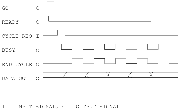
Device Interface - timing (non-burst mode)
SPD1,0: 0,0 0,1 1,0 1,1
GO, ACLO FNCT2
pulse widths: 100ns all speeds
END CYCLE
pulse width: 100ns all speeds
Cycle request to
input data latched: 200ns* 250ns* 300ns* 350ns*
Output data stable to
trailing edge of BUSY: 100ns 150ns 200ns 250ns
READY true to
trailing edge of BUSY: 90ns 140ns 190ns 240ns
Cycle request to
BUSY assertion: 150ns* all speeds
BUSY minimum width: 100ns 150ns 200ns 250ns
Minimum full handshake
time (cycle request to
BUSY end): 250ns 3000ns 350ns 400ns
Maximum full handshake time: system dependent
* Timings +/- 25ns
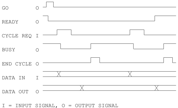
Device Interface - timing (burst mode output)
SPD1,0: 0,0 0,1 1,0 1,1
GO, ACLO FNCT2
pulse widths: 100ns all speeds
END CYCLE
pulse width: 50ns all speeds
Output data stable to
trailing edge of BUSY: 50ns 100ns 150ns 200ns
READY true to
trailing edge of BUSY: 50ns 100ns 150ns 200ns
Cycle request to
first BUSY assertion: 150ns* all speeds
BUSY minimum width: 50ns 100ns 150ns 200ns
BUSY minimum off time: 50ns all speeds
Minimum BUSY assertion
to BUSY assertion: 100ns 150ns 200ns 250ns
Maximum full handshake time: system dependent
* Timings +/- 25ns
Board dimensions: 10116 full size PCI
10118 half size PCI
External connector: board mounted 80-pin high-density SCSI-2 type connector AMP #749649-8
flat cable options use connectors compatible with above, in combination with 3M #3417 compatible male or female connectors round cable options use connectors compatible with the AMP part on each end
Power consumption:2.2A at +5V maximum
The 10116 and 10118 offer the same basic features and high performance. There are, however, differences between the two models, and within each model - as indicated by revision level. Note that revision level refers to the revision level reported in the board's configuration registers and on the EEPROM label, not to the artwork revision letter of the board itself.
The differences between the 10116 and 10118 are caused by the need to drop the local memory and internal pin strip connectors of the 10116 in order to fit the same high-performance core logic on a half-size PCI card. Because it has no local memory, the 10118 can't do chaining DMA when assembled with the PLX 9060 REV 3 chip. It will do DMA chaining from host memory when assembled with the 9080 chip. The FIFOs used are not part of local memory. Both the 10116 and 10118 carry 8Kbytes of FIFO for each transfer direction.
DMA byte swapping is not supported by the PLX 9060 REV 3 chip, it is supported by the 9080 chip.
10116 and 10118 boards that have PLD221G or later installed add Tahoma Burst Mode output (20Mbyte/second) and 0 wait state write capability. PLD221G is a socketed FPGA that will be installed on a board at customer request. Since it is an option, its presence is not reflected in the board’s EEPROM revision. Device drivers desiring to use these features should probe the Mode register’s BURST bit to verify the presence of PLD221G.
See the Tahoma Burst Mode and 0 Wait State Write sections of this manual for further information.
The availability of the PLX chips that both boards use has caused differences in features between rev levels within a given model:
10116 REV 0 Uses PLX 9060 REV 2 chip. Has no local memory. Requires special procedure to access DMA registers. Does not support DMA chaining. Does not support DMA byte swapping.
10116 REV 1 Uses PLX 9060 REV 3 chip. Has local memory. Has DMA chaining capability using local memory for DMA chain entries. DMA control/status registers must be accessed in the "IKON" register map. Does not support DMA byte swapping. Both DMA channels available ("A" artwork boards and later).
10116 REV 2 Never in production.
10116 REV 3 Uses PLX 9080 chip. Has local memory. Will do DMA chaining from local memory or host PCI memory. DMA control/status registers may be accessed in the "IKON" map, or directly in the "PLX" register space. Supports DMA byte swapping. Both DMA channels available.
10118 REV 0 Never in production.
10118 REV 1 Uses PLX 9080 chip. Has no local memory. Will do DMA chaining from host PCI memory only. DMA control/status registers may be accessed in the "IKON" map, or directly in the "PLX" register space. Supports DMA byte swapping. Both DMA channels available.
NOTE: The REV referred to above is the revision level reported in the board's configuration registers and on the EEPROM label, not the board's artwork revision level.
All current production of the 10116 and 10118 uses the PLX 9080-3 chip.
These chips are described in detail in documentation available from PLX Technology:
As of this writing:
9080 Revision 3 manual: 9080_105ds.pdf
9080 Revision 3 errata: 9080-3errata-13.pdf
The Model 10116/10118 includes three sets of registers: the PCI configuration registers, the bus interface chip run-time registers, and the "working" ("IKON") registers.
The working registers are referred to as “IKON” registers for compatibility with earlier documentation and software.
The PCI configuration registers are used to configure the board's slave addresses and ISA compatible interrupt level. These registers are configured by BIOS, using accesses in configuration space, to assign slave addresses to the register sets used by the 10116/10118. The configuration registers may be read by a device driver - using calls to BIOS PCI services - to determine what the assigned addresses are, and whether they are mapped into I/O or memory space.
The bus interface chip's run-time registers (and local configuration registers - which will in general not be used by the device driver) occupy 512 bytes (in the early release of the 10116, they occupy 256 bytes), and may be mapped into I/O and/or memory space. The chip indicates to BIOS that it supports both maps, and, in general, BIOS will allocate space in both maps. Configuration registers indicate where in the maps space has been allocated. The PLX chip permits BIOS to map its registers anywhere in 32 bit memory space. Typically, it will be mapped in to high memory, which is not directly accessible by an X86 type processor operating in real mode. In a DOS environment, DOS extenders will be required to access these registers in the memory map. If BIOS also maps the run-time registers into I/O space, simple I/O instructions may be used. The 10116/10118 also allows access to these registers in a portion of the "IKON" register map, which allows for simpler access, either via the I/O map, or in low memory, depending on the EEPROM installed in the 10116/10118. Access to the run-time registers is required when using interrupts or DMA.
For a reason known only to PLX, the DMA registers in the 9060 REV 3 chip are not directly accessible. They must be accessed via the "IKON" register map. The 9080 allows direct access to the DMA registers via the PLX register map.
The Model 10116/10118 "working" registers and DMA chain memory occupy an 8Kbyte block of addresses which may be located in high memory, low memory, or I/O space. The EEPROM installed on the 10116/10118 indicates to BIOS which map is to be used. The normal factory EEPROM allows mapping anywhere in memory space, which will normally cause BIOS to map the board into very high memory - requiring DOS extenders, or protected mode operation. Optionally, EEPROMs may be installed which will cause the board to be mapped into low memory or I/O space. Mapping into I/O space can simplify a driver, since simple X86 I/O instructions may be used to access the "IKON" registers (and the run-time PLX registers if BIOS has allocated space in the I/O map).
All on-board registers are organized as 32 bit words. The configuration and run-time registers are full 32 bit registers. All of the "IKON" registers, except the 16 bit Data Out and Data In registers, use only 8 bits - aligned as the low byte, on 32 bit boundaries.
NOTE: If the 10116/10118 is mapped into memory, and caching is enabled for that region of memory, care must be taken after writing to registers, to make sure that the cache has been written to the 10116/10118 before the next operation is begun.
It may be necessary to disable cache for the regions occupied by the 10116/10118's registers and memory. If that is not possible, doing a register read following a write may force the cache to drain. The approach taken will be determined by the characteristics of the specific system in which the 10116/10118 is installed.
All register addresses are in HEX.
Bit 31 is the MSB for all registers during 32 bit access. The run-time registers use all four bytes. All "IKON" registers, except the Data Out and Data In registers - which are 16 bits wide - use only the low byte. For those registers, only the low 8 bits are shown here.
The PLX registers shown here are representative of the registers supported by the PLX 9060, and 9080.
Current designs are based on the PLX 9080-3. Full documentation on these parts is available from PLX Technology:
Refer to PLX Technology (http://www.plxtech.com) for full descriptions of the PLX configuration and run-time registers.
As of this writing:
9080 Revision 3 manual: 9080_105ds.pdf
9080 Revision 3 errata: 9080-3errata-13.pdf
PCI Config Address |
Register Function |
|||
00h |
Device ID |
Vendor ID |
||
04h |
Status |
Command |
||
08h |
Class Code |
Revision ID |
||
0Ch |
BIST |
Header |
Latency |
Cache Line |
10h |
PCI Memory Base for Runtime Registers |
|||
14h |
PCI I/O Base for Runtime Registers |
|||
18h |
PCI I/O or Memory Base for “IKON” Registers |
|||
1Ch |
|
|||
20h |
|
|||
24h |
|
|||
28h |
|
|||
2Ch |
Subsystem Device ID |
Subsystem Vendor ID |
||
30h |
|
|||
34h |
|
|||
38h |
|
|||
3Ch |
Max Latency |
Min Grant |
Int Pin |
Int Line |
These registers are described in detail in documentation available from PLX Technology. For the most part, they are configured according to the parameters established by the 10116/10118's EEPROM, and by BIOS (or some equivalent mechanism, depending on host computer architecture). They may be accessed by a device driver by first asking BIOS if the board is present - by calling BIOS services with the board's Vendor ID (0x11D5) and Device ID (0x0116 or 0x0118). That call returns a “handle”. The “handle” is used in later BIOS calls to read the configuration registers.
The PCI memory base for runtime registers indicates where in the memory map the PLX chip's registers are located. This may be anywhere in memory. The PCI I/O base for runtime registers indicates where in I/O space these registers are located. Most BIOS implementations will assign areas in both spaces to the run-time registers. The early version of the PLX chip does not support direct access to the DMA control registers. The 10116/10118 allows access to these registers by doing a local bus write-back or read-back when these registers need to be accessed. The PLX runtime register set, including the DMA registers, are mapped into a portion of the "IKON" register map. Writes to this area cause an automatic local bus write-back. In the initial version of the 10116, reads cause a read from the desired register into a local holding register, which may then be read back at a specific location in the "IKON" map. In the early production 10116/10118, reads from the PLX registers via the "IKON" map will be direct, and will not use the PLX Run-Time Read Back register. In the final production versions of the boards (the ones available as of this writing), the DMA registers will also be directly accessible in the PCI space allocated for the PLX Runtime registers.
The PCI I/O or memory base for "IKON" registers indicates where the "IKON" registers are located, and in which map. The EEPROM tells BIOS whether the registers may be located in I/O, low memory, or high memory space.
The only other register normally of use to the device driver is the Int Line. The 10116/10118 is always connected to PCI INT A. This interrupt may be assigned by BIOS to an ISA-type interrupt level, which is reported in this register, and should be used by the driver when handling interrupts from the 10116/10118.
The address shown in parentheses is the offset into the "IKON" register set.
PCI Runtime Offset (“IKON” Offset) |
Register Function |
00h (80h) |
Range for PCI to “IKON” Registers |
04h (84h) |
Re-map for PCI to “IKON” Registers |
08h (88h) |
Local Arbitration Register (9080 only) |
0Ch (8Ch) |
Big/Little Endian Register (9080 only) |
10h (90h) |
Range for Expansion ROM (not used) |
14h (94h) |
Re-map for ROM (not used) & BREQ Control |
18h (98h) |
Bus Region Descriptors |
1Ch (9Ch) |
Range for Direct Master (not used) |
20h (A0h) |
Local Base for Direct Master (not used) |
24h (A4h) |
Local Base for Direct Master (not used) |
28h (A8h) |
PCI Re-map for Direct Master (not used) |
2Ch (ACh) |
PCI Configuration for Direct Master (not used) |
These registers are described in detail in documentation available from PLX Technology. They are set to appropriate values by the EEPROM on the 10116/10118, and should not be modified by the device driver.
PCI Runtime Offset (“IKON” offset) |
Register Function |
|
40h (C0h) |
Mailbox Register 0 (not used) |
|
44h (C4h) |
Mailbox Register 1 (not used) |
|
48h (C8h) |
Mailbox Register 2 (not used) |
|
4Ch (CCh) |
Mailbox Register 3 (not used) |
|
50h (D0h) |
Mailbox Register 4 (not used) |
|
54h (D4h) |
Mailbox Register 5 (not used) |
|
58h (D8h) |
Mailbox Register 6 (not used) |
|
5Ch (DCh) |
Mailbox Register 7 (not used) |
|
60h (E0h) |
PCI to Local Doorbell Register (not used) |
|
64h (E4h) |
Local to PCI Doorbell Register (not used) |
|
68h (E8h) |
Interrupt Control/Status |
|
6Ch (ECh) |
EEPROM Control & User I/O Bits |
|
70h (F0h) |
Device ID |
Vendor ID |
74h (F4h) |
Unused |
Revision ID |
These registers are described in detail in documentation available from PLX Technology. The only functions used in these registers will be the Interrupt Control/Status bits.
PCI Runtime Offset (“IKON” Offset) |
Register Function |
80h (100h) |
DMA Channel 0 Mode |
84h (104h) |
DMA Channel 0 PCI Address |
88h (108h) |
DMA Channel 0 Local Address |
8Ch (10Ch) |
DMA Channel 0 Transfer Count |
90h (110h) |
DMA Channel 0 Descriptor Pointer |
94h (114h) |
DMA Channel 1 Mode |
98h (118h) |
DMA Channel 1 PCI Address |
9Ch (11Ch) |
DMA Channel 1 Local Address |
A0h (120h) |
DMA Channel 1 Transfer Count |
A4h (124h) |
DMA Channel 1 Descriptor Pointer |
A8h (128h) |
DMA Command/Status Register |
ACh (12Ch) |
DMA Arbitration Register 0 |
B0h (130h) |
DMA Arbitration Register 1 |
These registers are described in detail in documentation available from PLX Technology. They will be used by the device driver to set up and initiate DMA (bus master) transfers between PCI memory and the 10116/10118's FIFOs. Early versions of the 10116 require accessing the DMA registers as part of the "IKON" register map. Later boards also allow access to the DMA registers in the PLX run-time register map. The early versions of the PLX chip did not allow direct host access to the DMA registers. Logic on the board allows accessing these registers via host accesses in a portion of the "IKON" map. These accesses are converted to local bus accesses to the PLX chip. See the DMA operation section of this manual for information on how to access the DMA registers in early versions of the board.
NOTE: The 10116/10118 was originally designed to use DMA channel 0 of the PLX 9060. Because of some early bugs in the PLX chip (which did not affect Tahoma Technology's designs) some PLX customers elected to use DMA channel 1 for single DMA channel designs, which became the only channel supported in some PLX chips (the 9060 SD).
The 10116/10118 DMA request logic is connected to both channels of the PLX chip. Code written for either channel will work correctly. Tahoma recommends writing new code for DMA channel 1.
All offsets are from the "IKON" memory or I/O space base address.
Offset |
Register Function |
read/write |
00h |
Latched Functions |
read/write |
04h |
116/118 Pulses |
write only |
04h |
Flags |
read only |
08h |
Device Pulses |
write only |
08h |
Status |
read only |
0Ch |
Mode |
read/write |
10h |
Range Count Low Byte |
read/write |
14h |
Range Count Middle Byte |
read/write |
18h |
Range Count High Byte |
read/write |
1Ch |
FIFO Status |
read only |
40h |
Data Out |
write only |
50h |
0 Wait State Data Out (* see Note A) |
write only |
40h |
Data In |
read only |
60h |
PLX Run-time Read Back |
read only |
80h-13Fh |
PLX Run-time Registers |
read/write |
140h-1FFFh |
Local Chain Memory (** see Note B) |
read/write |
These are the registers of primary interest to the device driver. All are 8 bits wide aligned as the low bytes of 32 bit words, and may be accessed as 8, 16, or 32 bit values, except the 16 Bit Data Out and Data In registers. The PLX registers may be accessed as 8, 16, or 32 bit values. The 16 Bit Data Out register may be written as 16, or 32 bits, but only the low 16 bits will be used. The 16 bit Data In register may be read as 16 or 32 bits, but only the low 16 bits will be valid.
* Note A The 0 Wait State Data Out address is available only on boards using PLD221G or later. It must only be used for DMA output, and only when the DMA channel is configured for 0 wait states. PLD221G also added Tahoma Burst Out capability. These functions may be tested for by probing the BRST bit in the mode register. See the Mode Register description in this document. See also the 0 Wait State Write and Tahoma Burst Mode Output sections of this manual.
** Note B Not available on the 10118. Chain lists (if used) in PCI host memory.
Bit |
Name |
Function |
07 |
EORM |
End of Range Interrupt Mask |
06 |
ATTM |
Attention Interrupt Mask |
05 |
DMON |
Enable DMA Requests |
04 |
DMIN |
Data Direction Control |
03 |
FCN3 |
Function Bits |
02 |
FCN2 |
|
01 |
FCN1 |
|
00 |
0 |
Reserved |
These latched bits control several functions internal and external to the 1011610118. They are reset to zero by a bus initialize or by MCLR (master clear) in the 116/118 Pulses Register.
EORM This bit enables the end of range flag - EORF in the Flags Register - to cause an interrupt. EORF is set when the DR11 range counter underflows at the end of a DR11 block transfer.
ATTM This bit enables the attention flag - ATTF in the Flags Register - to cause an interrupt. ATTF is set on a false to true transition of the ATTENTION input.
EORM and ATTM control interrupts from the "IKON" portion of the 10116/10118. It is also necessary to enable interrupts in the PLX chip by setting bit 11 (PCI local interrupt enable) to 1 in the Interrupt Control/Status register, and leaving bit 8 (PCI interrupt enable) at its default state (set). DMA done can also cause an interrupt. See the Interrupts section of this manual for further information.
DMON DMON enables the "IKON" portion of the logic to request DMA service from the PLX chip. The PLX DMA registers should be set up for DMA transfers before setting this bit.
DMIN This bit controls the direction of DR11 block transfers (DMA) in the "IKON" portion of the 10116/10118. The transfer direction must also be set in the PLX DMA control registers before beginning a DMA transfer.
For output (data from PCI memory to the attached device), DMIN = 0. For input (data from attached device to PCI memory), DMIN = 1.
This bit is used instead of the external input signal C1 CONTROL, which sets transfer direction on DEC DR11s.
NOTE: DMIN must be set to the appropriate state (for input or output) prior to enabling DMA transfers with DMON, or issuing a GO pulse.
FCN3,2,1 These latched bits are presented to the attached device. They may be used for any purpose. In interprocessor links, their meanings are defined by the cable and connector pin-outs. See the Interprocessor Links section of this manual for further information.
Bit |
Name |
Function |
07 |
REOR |
Reset End of Range Flag |
06 |
RATN |
Reset Attention Flag |
05 |
RERR |
Reset Error Flag |
04 |
MCLR |
Master Reset “IKON” Logic |
03 |
CLOF |
Clear Output FIFO |
02 |
CLIF |
Clear Input FIFO |
01 |
RDOF |
Read Output FIFO |
00 |
WRIF |
Write Input FIFO |
The bits in the 116/118 Pulses Register are used to provide internal pulsed functions. Writing a 1 to a bit in this register pulses the associated function. Writing a 0 has no effect. It is not necessary to clear a 116/118 Pulses Register bit to 0 after setting it to 1.
REOR Resets the end-of-range flag (EORF) and its associated interrupt.
RATN Resets the ATTENTION flag (ATTF) and its associated interrupt.
RERR Resets the parity error (PERR) and Multi Cycle Error (MCER) flags. These flags do not cause interrupts or interfere with data transfer although the condition flagged may result in corrupted data.
MCLR Initializes the "IKON" portion of the 10116/10118 and clears the input and output FIFOs. MCLR does not send an INIT signal to the attached device.
CLOF Clears the output FIFO, and sets it to empty status.
CLIF Clears the input FIFO, and sets it to empty status.
RDOF This pulse causes the next 16 bit data word in the output FIFO to be written to the output latches - where it will be visible to the external device. This bit does not cause any change in the control signals to the attached device.
WRIF This pulse causes the data present on the input lines from the attached device to be written to the next available location in the input FIFO. It does not cause any change in the control signals to the attached device.
RDOF and WRIF are used in combination with the Data Out and Data In registers to provide a programmed I/O path to and from the attached device. They are NOT used during DMA transfers. To write a 16 bit value to the output data lines, the program would first write the appropriate data to the Data Out Register, and then pulse RDOF. Similarly, to read the input data lines, the program would first pulse WRIF, and then read the Data In register. In both cases, the program should clear the associated FIFO before and after performing the read or write operation.
In general, the program should deal with 16 bit transfers to and from the output and input data lines as "monolithic" operations. It is not possible, for instance, to pulse WRIF ten times, and then read the Data In register ten times, and expect ten valid reads. The program should clear the input FIFO, pulse WRIF once, read the Data In register, and clear the input FIFO again. The PLX chip always does 32 bit read transfers, and will read extra data from the input FIFO. This is not a problem as long as programmed I/O data transfers are "monolithic".
Bit |
Name |
Function |
07 |
EORF |
End of Range Flag |
06 |
ATTF |
Attention Flag |
05 |
PERR |
Parity Error Flag |
04 |
MCER |
Multi-cycle Error Flag |
03 |
0 |
reserved |
02 |
0 |
reserved |
01 |
0 |
reserved |
00 |
0 |
reserved |
The bits in the Flags Register indicate the states of various internal flags. All bits in this register are cleared to 0 at system power-up, or by pulsing MCLR in the 116/118 Pulses Register.
EORF This bit sets when the 10116/10118's range counter underflows. (The range counter controls the DR11 block length, not the individual DMA block length.) EORF will stay set until reset by pulsing REOR or MCLR in the 116/118 Pulses Register. It is also cleared by a bus initialize. IF EORF and its interrupt mask bit (EORM in the Latched Functions Register) are both set (and the appropriate bits in the PLX chip are set) an interrupt will be requested.
NOTE: See the EOR Note below for information on EORF interrupt hold off.
ATTF This bit sets on the rising edge of the ATTENTION H input signal from the attached device. ATTF will stay set until reset by pulsing RATN or MCLR in the 116/118 Pulses Register. If ATTF and its interrupt mask bit (ATTM in the Latched Functions Register) are both set an interrupt will be requested.
NOTE: See the EOR Note below for information on ATTF interrupt hold off.
PERR PERR is set by any parity error detected during DMA or Programmed-I/O input from the external device. It will stay set until reset by RERR or MCLR in the 116/118 Pulses Register. It is also cleared by a bus initialize. The parity check indicated by PERR applies only to data on the external cable, not to any bus or system data. PERR is a status bit only, and does not halt, terminate, or otherwise affect data transfers.
Please note that external parity checking is currently only supported by Tahoma Technology's DR11 emulator family (although the Sbus board - the 10103, does not support parity), and will be useful only in links with those products. In general, when connected to another manufacturer's DR11, or compatible device, PERR will set frequently. In these applications it should be ignored by the software.
MCER Indicates a multi cycle error during block transfers. This bit sets if a cycle request is received while BUSY is still asserted. In this case, the transfer requested by the offending cycle request will probably be ignored, and the data is almost certainly corrupted. This bit is most useful when collecting data that is strobed in at fixed intervals, and can't be held off by BUSY. MCER indicates that the 10116/10118 and/or system bus has not been able to keep up with the incoming data. It is a status bit only, and does not cause an interrupt or inhibit further data transfers.
MCER will stay set until cleared by RERR or MCLR in the 116/118 Pulses Register. It is also cleared by a bus initialize.
EOR NOTE: When in input mode EORF sets at the beginning of the last DR11 input cycle. At this time, there may or may not be data in the FIFO buffers. ATTF and EORF interrupts will be held off until the input FIFO has been drained to memory. FIFO draining will begin when READY goes true following end of range or ATTENTION. The interrupts are held off to assure that all data is in memory (and the 10116/10118 is idle) before interrupt code is executed. The REDY bit is also held at 0 until the input FIFOs are empty.
Input block transfer completion should be determined by the DMA done interrupt, the ATTF interrupt, or by polling REDY. At the time that the interrupt hold-off ends (when the input FIFO goes empty), there may still be a small amount of data in the PLX chip's internal DMA FIFO. This should not be more than a few 32 bit words, and should drain to memory very quickly (in a few hundreds of nanoseconds). If desired, the program can verify that the PLX FIFOs have drained by examining the DMA channel 0 (or channel 1, if that is the channel being used) done bit in the DMA Command/Status Register in the PLX Runtime Registers. Using the PLX DMA done interrupt avoids these issues. The interrupt is not issued until all data has been transferred to memory.
In output mode, EORF sets at the beginning of the last DR11 transfer cycle. The EORF interrupt, if enabled, is held off until the end of the cycle. In the unlikely event that the last output cycle begins when there is no data in the output FIFO, the interrupt and the REDY bit will be held off until data becomes available, and the transfer is complete. Completion of an output block transfer should be determined via the EORF interrupt, or by polling REDY, not by polling EORF.
Bit |
Name |
Function |
07 |
SRDY |
Terminate Block - Force READY |
06 |
|
reserved |
05 |
|
reserved |
04 |
INIT |
Pulse INIT to Device |
03 |
|
reserved |
02 |
ACF2 |
Pulse ACLO FNCT2 to Device |
01 |
CYCL |
Force CYCLE REQUEST |
00 |
GO |
Pulse GO - Enable Block Transfer |
The bits in the Device Pulses Register are used to provide external pulsed functions. Writing a 1 to a bit in this register pulses the associated function. Writing a 0 has no effect. It is not necessary to clear a Device Pulses Register bit to 0 after setting it to 1.
SRDY Pulsing this bit forces REDY true, and terminates the block transfer. If the transfer was an input, and there is data in the input FIFO, it will be drained to PCI memory. SRDY is not actually an external pulse, but does affect the external READY H signal.
INIT This causes a 100ns pulse on the INIT H signal to the attached device.
ACF2 ACF2 causes a 100ns pulse on the ACLO FNCT2 signal to the attached device. Setting FCN2 in the Latched Functions Register will also force ACLO FNCT2 high.
CYCL This bit duplicates the effect of an external cycle request. Pulsing CYCL after, or at the same time as GO, causes an input or output cycle to begin immediately. It is typically used to start an output block handshake in an interprocessor link, or to start input or output when in loopback mode.
GO This bit causes a 100ns pulse on the GO signal to the attached device, and enables the 10116/10118 to accept cycle requests.
Bit |
Name |
Function |
07 |
REDY |
READY |
06 |
ATTN |
ATTENTION Input |
05 |
0 |
reserved |
04 |
0 |
reserved |
03 |
STTA |
Status Bits From Device |
02 |
STTB |
|
01 |
STTC |
|
00 |
A00 |
A00 Input From Device |
The bits in this register reflect Ready status, and the states of input signals from the attached device.
REDY REDY follows the READY H signal to the attached device. REDY being true (a ONE) indicates that the 10116/10118 is idle, and can accept a GO command. REDY false indicates that a GO command has been issued, and that block transfers are enabled. REDY - and READY H - is cleared by GO, and set by SRDY or MCLR in the Pulses Register, a bus initialize, range counter underflow (provided that RDIS is 0), or ATTENTION.
REDY will stay false following a block input operation until the input FIFOs have been drained to memory. REDY may be monitored following a SRDY pulse, end-of-range, or ATTENTION to determine when all data has been input. EORF should not be used to determine the end of an input operation, as it will set when the last word is written to the FIFOs, not when the last word is drained to memory.
This also applies to output, in which case REDY will be held off until the last output cycle has completed, even though end of range occurs at the beginning of the last cycle.
ATTN ATTN follows the state of the ATTENTION H input from the attached device. ATTENTION will terminate a block transfer, and cause an interrupt, if enabled. In interprocessor links, ATTENTION is often used to indicate that the "far end" of the link is ready for a block transfer. The program at the "near end" would typically wait for ATTENTION (by monitoring ATTF in the Flags Register, or by enabling an ATTF interrupt), and then issue GO to start the transfer. Since ATTENTION aborts a block transfer, GO must not be issued while ATTENTION is still true. The ATTN bit may be monitored to ensure that ATTENTION is false when GO is issued.
STTx The STTA, B, and C bits follow the states of the STATUSA, B, and C inputs from the attached device. They have no direct effect on the 10116/10118, and may be used by the application as appropriate. Most interprocessor link applications follow the STATUSx and FNCTx usage conventions suggested by the DEC DR11-W user's guide.
A00 The A00 bit is a status bit that indicates the state of the A00 input from the attached device. A00 is not used by the 10116/10118, which does not allow external byte DMA requests, but is made available as a diagnostic input. It may also be useful in interprocessor link applications, as it will indicate the state of the other DR11's READY H output. It should be noted that a readable A00 input is not always available in other DR11s and emulators.
Bit |
Name |
Function |
07 |
LRDY |
Enable Long READY |
06 |
RDIS |
Disable Range Counter |
05 |
BDIS |
Disable CYCLE REQUEST B input |
04 |
BRST |
Enable Tahoma Burst Mode Output (* see note A) |
03 |
CRQP |
CYCLE REQUEST Polarity |
02 |
BSYP |
BUSY Polarity |
01 |
SPD1 |
Handshake Timing Selection |
00 |
SPD0 |
These latched bits control several functions internal and external to the 10116/10118. They are reset to zero by a bus initialize or by MCLR (master clear) in the 116/118 Pulses Register.
* Note A Only available on board with PLD221G or later installed. See BRST bit description below, and Tahoma Burst Mode Output section of this manual.
LRDY The standard DR11-W handshake protocol requires that READY H go true during the last BUSY assertion of the block. If LRDY is zero, the 10116/10118 will set READY H true during the last BUSY of the block. If LRDY is a one, READY H will go true simultaneously with the trailing edge of the last BUSY of the block. If normal READY timing is selected, the amount of time prior to the trailing edge of BUSY that READY H is asserted depends on the handshake timing selected.
RDIS Setting RDIS to one disables the 10116/10118's DR11 range counter. Normally, when the DR11 range count underflows, READY H goes true, and the block transfer is terminated. If RDIS is set to one, the range counter is disabled, and continuous data collection is possible. The on-board FIFOs allow data collection to continue, even between DMA blocks.
BDIS This rarely-used bit duplicates the effect of grounding the CYCLE REQ B input. A DR11-W normally will respond to transitions on either the CYCLE REQ A or B input, as long as the other input is held low. Most applications, including interprocessor links, ground CYCLE REQ B by virtue of the cable pin-out. For the unusual case that leaves it floating, BDIS can be used to hold CYCLE REQ B at a logic low. Note that this is done internally - the input is not actually grounded.
BRST Boards with PLD221G or later installed are capable of 20Mbyte/second burst output. This mode of operation requires that the attached device also support Tahoma Burst Mode Output; it is not useable with normal DR11-W type devices. In this mode the Cycle Request input is used for flow control rather than as a word-by-word handshake signal. See the Tahoma Burst Mode Output section of this manual for details.
PLD221G also introduces 0 (zero) Wait State output FIFO writes. If this mode is enabled during DMA output, the output FIFO is written at 40Mbytes/second (normal DMA output writes data to the FIFO at 20Mbytes/second). This can be an advantage in any application, as it helps keep the output FIFO loaded with data. It is a particular advantage when using Tahoma Burst Mode Output, since it allows DMA FIFO writes to “keep ahead” of the 20Mbyte/second device transfer rate, even in the presence of other PCI bus traffic. To use 0 wait state writes, DMA must be set up accordingly, and a different local bus target address used. See the 0 Wait State Write section of this manual for details.
The BRST bit should be probed to verify the presence of PLD221G on the board. If a 1 is written to this bit, it will read back as a 0 if PLD221G is not present, and 1 if it is.
CRQP CRQP controls which edge of the cycle request input(s) is active. Interprocessor links, and most applications, require that cycle requests be active on the rising edge of the input used. CRQP = 0 causes cycle requests to be rising edge active. CRQP = 1 makes the cycle request inputs falling edge active.
If Tahoma Burst Mode Output is enabled, the cycle request inputs become level-sensitive flow control inputs. Polarity is still selectable. See the Tahoma Burst Mode Output section of this manual for details.
BSYP Interprocessor link mode, and many applications, require BUSY to be asserted low. Some applications (in what DEC calls "Device Mode") require a high BUSY assertion. BSYP = 0 causes BUSY to be asserted low. BSYP = 1 causes BUSY to be asserted high.
SPD1,0 These bits control the four possible handshake timings uses when doing block transfers to and from the attached device. The choices allow tuning the connection for the highest possible throughput, while still allowing for slowing down when necessary to meet specific device or cable requirements.
Selecting Tahoma Burst Mode Output changes the meaning of these bits for output only. See below and the Tahoma Burst Mode Output section of this manual for details.
Non-burst mode timing (BRST = 0) input/output::
SPD1,0: 0,0 0,1 1,0 1,1
GO, ACLO FNCT2
pulse widths: 100ns all speeds
END CYCLE
pulse width: 100ns all speeds
Cycle request to
input data latched: 200ns* 250ns* 300ns* 350ns*
Output data stable to
trailing edge of BUSY: 100ns 150ns 200ns 250ns
READY true to
trailing edge of BUSY: 90ns 140ns 190ns 240ns
Cycle request to
BUSY assertion: 150ns* all speeds
BUSY minimum width: 150ns 200ns 250ns 300ns
Minimum full handshake
time (cycle request to
BUSY end): 300ns 350ns 400ns 450ns
Maximum full handshake time: system dependent
* Timings +/- 25ns
Burst mode timing (BRST = 1) output only:
SPD1,0: 0,0 0,1 1,0 1,1
GO, ACLO FNCT2
pulse widths: 100ns all speeds
END CYCLE
pulse width: 50ns all speeds
Output data stable to
trailing edge of BUSY: 50ns 100ns 150ns 200ns
READY true to
trailing edge of BUSY: 50ns 100ns 150ns 200ns
Cycle request to
first BUSY assertion: 150ns* all speeds
BUSY minimum width: 50ns 100ns 150ns 200ns
BUSY minimum off time: 50ns all speeds
Minimum BUSY assertion
to BUSY assertion: 100ns 150ns 200ns 250ns
Maximum full handshake time: system dependent
* Timings +/- 25ns
Register Offset |
18h |
14h |
10h |
Register Bits |
7 - 0 |
7 - 0 |
7 - 0 |
Range Bits |
23 - 16 |
15 - 8 |
7 - 0 |
The Range Count Register is a 24 bit counter that controls the number of 16 bit words transferred to or from the attached device.
Prior to pulsing GO in the Device Pulses Register, the Range Count Register is loaded with the number of 16 bit DR11 words to be transferred minus 1. It will decrement by one with each word transferred. When it underflows, the READY H output will be set to one, and further cycle requests from the external device will be ignored. The end-of-range flag (EORF in the Flags Register) will also be set, and will cause an interrupt if enabled.
NOTE: Unlike the some other DR11s, the 10116/10118 does not always set REDY in the Status register at the same time that the READY H output is asserted. At the end of a DR11 output block, the READY H output goes true at the beginning of the last DR11 cycle. The REDY bit does not set until the last transfer is complete. This normally occurs in a few tens of nanoseconds, but may take longer in the unlikely event that the output FIFO is empty when the last transfer begins.
In input mode REDY does not set until all data in the input FIFO has been drained into the PLX chip’s internal FIFO.
The interrupts (potentially) caused by the EORF and ATTF flags are held off until the last output transfer is complete, or all input data has been drained to memory. This guarantees that at interrupt time, or when REDY sets in polling mode, that output is complete, or that all input data is available in memory, and the program can safely touch the registers on the 10116/10118.
In input mode, the small PLX FIFO can contain a few longwords when REDY and the interrupt go true. This FIFO drains to memory very rapidly, and it is nearly impossible that it will not be empty by the time the interrupt is processed, or the poll is acted upon. To be absolutely certain that all data is in memory after a DMA input, PLX DMA done status should be checked. In fact, most drivers will use the PLX DMA done interrupt when in input mode, which avoids this problem.
This counter does not directly control the DMA transfer count. That is set in the PLX chip's registers. Several DMA blocks (using either chaining or program intervention) may be used to satisfy the Range Count Register's starting count. This will be useful when the attached device's required number of words per DR11 block exceeds the maximum available or desired in a single DMA block. In general, the total number of words requested in multiple DMA blocks should match the word count in the Range Count Register.
Please note that the initial value entered in the Range Count Register is always the WORD count minus 1.
Bit |
Name |
Function |
07 |
FOFF |
Output FIFO Full |
06 |
FOHF |
Output FIFO Half Full |
05 |
FOEF |
Output FIFO Empty |
04 |
0 |
reserved |
03 |
FIFF |
Input FIFO Full |
02 |
FIHF |
Input FIFO Half Full |
01 |
FIEF |
Input FIFO Empty |
00 |
0 |
reserved |
This register indicates the status of the input and output FIFOs. It is primarily diagnostic in nature and will probably not be used in normal operation.
The Data Out register is used in conjunction with the 116/118 Pulses register to write individual 16 bit words to the attached device. Data written to this register is entered into the output FIFO. Data will generally be written 16 bits at a time - to match the width of the DR11 output data path. This register may be written as a 16 or 32 bit value. If written as a 32 bit value, only the lower 16 bits will be used.
Once in the FIFO, the RDOF (read output FIFO) bit in the 116/118 Pulses register can be used to write the data from the FIFO to the output data latches which drive the DO00-15 H output data lines. Again, it is possible to perform this operation multiple times to read multiple words from the FIFO, but this will generally not be done in practice.
It is good practice to use the CLOF bit in the 116/118 Pulses register to clear the output FIFO prior to using the Data Out register, to ensure that "left over" data in the FIFO is not presented to the external device inadvertently.
Data passed to the attached device in this way is presented on the output data lines immediately, without manipulation of any handshake signals. It does not duplicate block output handshaking (DMA). It is usually used in conjunction with the ACF2 pulse in the Device Pulses register to send a single word to the attached device, or other DR11 (or emulator).
Odd parity over 17 bits is maintained for output data. The 17th bit (POXX H) replaces a GROUND pin in the DEC DR11-W specification. Its use is optional.
NOTE: The output FIFO is used during DMA output. Writing to the Data Out register, or pulsing the RDOF bit during DMA output will cause data corruption.
NOTE: For programmed I/O output via the Data Out register, the 0x40 (40h) register offset must be used. The 0x50 (50h) address is only used for 0 wait state DMA output.
Reading the Data In register reads the next 16 bit value from the input FIFO. The data in the FIFO is normally entered from the DI00-15 H data in lines by pulsing the WRIF bit in the 116/118 Pulses register. It is good practice to first clear the input FIFO by pulsing the CLIF bit in the 116/118 Pulses Register. It is not possible to read multiple, valid, 16 bit words from the Data In Register. The PLX PCI interface chip always does a "read ahead" when a slave read is initiated by the host CPU. Additional words read "ahead" are discarded at the end of the read, and that FIFO data would be lost. This register may be read as a 16 or 32 bit value. When read as a 32 bit value, only the low 16 bits are valid.
Data read in this way does not use the block transfer handshake lines. It is generally used in conjunction with the ATTF bit in the Flags register as a way to read a single word from the attached device or other DR11.
Odd parity over 17 bits is checked during Programmed-I/O and DMA reads of the input data signals. The 17th bit (PIXX H) replaces a GROUND pin in the DEC DR11-W specification. Its use is optional. Input parity errors will cause PERR to set in the Flags Register, but will not affect an on-going transfer. When the 10116/10118 is connected to a device that does not generate parity on the DR11 cable (most do not) the PERR flag will set frequently. It should be ignored in these cases.
NOTE: The input FIFO is used during DMA input. Reading the Data In register, or pulsing the WRIF bit during DMA input will cause data corruption.
PLX Run-Time Read Back Read Only
This register is used in conjunction with the PLX Run-Time Registers portion of the "IKON" registers. Early versions of the PLX chip do not allow direct host access to the DMA registers. In order to read a DMA register (and optionally any other run-time register) it is necessary to first issue a read to the appropriate address in the PLX Run-Time Registers portion of the "IKON" map. This causes a local bus cycle that reads the selected register and holds it in a 32-bit holding register. That value may be read by accessing the PLX Run-Time Read Back register.
Only the initial release of the 10116 (EEPROM REV 0) will require using the PLX Run-Time Read Back register described above. Production 10116/10118 boards that use the PLX 9060 REV 3 chip will still require accessing the DMA (and optionally Run-Time) registers via the "IKON" map, but the reads will provide the desired register data directly, without using the read back register. The version of the PLX chip (the 9080) currently used in production allows direct access of the DMA registers in the PLX address space.
PLX Run-Time Registers Read/Write
This portion of the "IKON" register map is used to access the PLX chip's DMA registers, and optionally, the other PLX Run-time registers. Issuing a write to a register in this map causes an automatic local bus cycle that addresses the specified register and completes the write. This is the only way to access the DMA registers in early versions of the PLX chip. In the initial version of the 10116 (EEPROM REV 0), to read a register in this map, first do a dummy read to the desired address, and then read the actual value from the PLX Run-Time Read Back register. The production version of the 10116/10118 - using the 9060 REV 3 or 9080 - will provide the register data in the initial read, without requiring access to the read back register. Boards using the 9080 will also allow access to PLX Run-Time Registers in the PLX map.
On the 10116, this portion of the "IKON" map allows access to approximately 8K bytes of local memory. Early and intermediate releases of the PLX chip require that DMA command blocks ("chains", or "links") be in local bus memory when DMA chaining is used. The version of the PLX chip used in current production (the 9080) allows DMA chains to be in PCI host memory.
The 10118 has no local memory. DMA chaining is possible only from host memory - and only on versions of the board using the PLX 9080 chip. All versions of the 10118 can do single block DMA transfers. As of this writing, all production 10118 boards use the PLX 9080.
DMA chaining control blocks must be aligned on quad longword boundaries. See the DMA Operation section of this manual for further information.
NOTE: The 9060 REV 3, and 9080 chips provide both DMA channels 0 and 1. The board’s logic connects the DMA request signal to both channels. It is recommended that device driver code be written for channel 1, which avoids some issues with DMA channel 0 in certain PLX parts (the 9060 SD).
The 10116/10118 can operate as a 32 bit bus master. It is capable of transferring data to or from PCI memory at the full specified 132Mbtes/second into or out of the PLX chip's (small) FIFOs, and from there into or out of the on board FIFOs at approximately 20Mbytes/second (40Mbytes/second in 0 wait state write mode). The maximum rate to or from the attached device is 8Mbytes/second in normal DR11-W mode, and 20Mbytes/second with Tahoma Burst Mode Output.
FIFO depth is 8Kbytes each for both input and output. This can be increased as a factory option.
It is up to the application or device driver programmer to determine whether the PLX chip's DMA logic should be set up prior to, or after enabling the DR11-side logic. If a single DMA block transfer is to be used to satisfy the DR11 range count, typically, the DMA logic would be set up first. If multiple DMA blocks will be used, it is more likely that the DR11-side will be enabled first, and then the DMA logic.
Generally, the program will first write the appropriate word count minus 1 to the 10116/10118's Range Count Register. All 24 bits of the counter must be appropriately set. Then the bits of the Latched Functions Register would be set appropriately - device dependent function bits, transfer direction control (DMIN), and interrupt masks if desired. Finally, bits of the Device Pulses Register would be written, pulsing GO, CYCL if appropriate, and possibly ACF2. If the DMA logic has not been previously set up and enabled, it should be at this point. If all goes well, DMA will run to completion, setting the Channel 1 or 0 Done bit in the DMA Command/Status Register, and the end-of-range flag (EORF) in the Flags Register, if the transfer was to be done with a single DMA block. If multiple DMA blocks are required, the system's DMA logic would be set up and enabled again.
NOTE: The DMON bit in the Latched Functions Register does not automatically clear at the end of a DMA block. It is necessary to reset it following the completion of a DR11 block transfer, or unpredictable behavior may occur at the beginning of the next DR11 block.
During output, Channel 1 (or 0, depending on the channel used) Done will set before EORF. During input, EORF will set before Channel 1 (or 0) Done. Both may be set by the time an interrupt service routine is entered.
NOTE: Unlike the some other DR11s, the 10116/10118 does not always set REDY in the Status register at the same time that the READY H output is asserted. At the end of a DR11 output block, the READY H output goes true at the beginning of the last DR11 cycle. The REDY bit does not set until the last transfer is complete. This normally occurs in a few tens of nanoseconds, but may take longer in the unlikely event that the output FIFO is empty when the last transfer begins.
In input mode REDY does not set until all data in the input FIFO has been drained into the PLX chip’s internal FIFO.
The interrupts (potentially) caused by the EORF and ATTF flags are held off until the last output transfer is complete, or all input data has been drained to memory. This guarantees that at interrupt time, or when REDY sets in polling mode, that output is complete, or that all input data is available in memory, and the program can safely touch the registers on the 10116/10118.
In input mode, the small PLX FIFO can contain a few longwords when REDY and the interrupt go true. This FIFO drains to memory very rapidly, and it is nearly impossible that it will not be empty by the time the interrupt is processed, or the poll is acted upon. To be absolutely certain that all data is in memory after a DMA input, PLX DMA done status should be checked. In fact, most drivers will use the PLX DMA done interrupt when in input mode, which avoids this problem.
In the event of an incomplete or aborted transfer (any in which the range count is not exhausted) the SRDY bit in the Device Pulses Register should be pulsed to set READY H and the REDY bit, and the DMON bit in the Latched Functions Register should be cleared, and the Abort bit set in the DMA Control/Status Register to terminate DMA.
The Clear Input or Output FIFO bit(s) in the 116/118 Pulses Register may be used to insure that nothing is left in the FIFO buffers that might corrupt subsequent transfers. If SRDY is pulsed following an incomplete input, any data in the input FIFOs will be drained to memory, after which time DMA may be disabled. The REDY bit will set when the FIFOs have been emptied, and any interrupt caused by the EORF or ATTF flags will also be held off until the FIFOs are empty. If it is necessary to flush the input or output FIFOs - to the bit bucket - the master clear (MCLR) or FIFO clear (CLIF or CLOF) bit(s) should be used. MCLR will also reset other logic on the 10116/10118.
SRDY is also useful to re-set (to 1) READY H and the REDY bit following a GO which did not lead to DMA transfers. Some applications and devices use GO as a non-DMA command. The software driving the 10116/10118 can accommodate these applications by simply not enabling DMA when pulsing GO. SRDY should be used following the completion of this type of operation.
NOTE: The following discussion refers to DMA setup when using 1 wait state reads and writes. Boards with PLD221G and later installed are capable of doing 0 wait state output FIFO writes at 40Mbytes/second during DMA output. The presence of PLD221G may be determined by probing the BRST bit in the mode register. Use of the 0 wait state write mode is optional. See the Tahoma Burst Mode Output and 0 Wait State Write sections of this manual for further information.
DMA transfers are initiated by setting up and enabling the DMA (and interrupt) control logic in the PLX chip in addition to setting the transfer direction (DMIN) and DMA enable (DMON) in the "IKON" Latched Functions Register. The 10116/10118 can use whichever DMA channel is supported by the installed PLX chip. The PLX 9060 REV 3 supports channels 0 and 1. The PLX 9060 SD (not currently used in Tahoma products) has a single channel, which PLX chose to implement as channel 1. The PLX 9080 supports both DMA channels. Tahoma Technology recommends that device drivers use DMA channel 1. This discussion will refer to DMA channel 1. Non chaining DMA is accomplished by selecting non chaining mode in the DMA channel 1 Mode register. The Channel 1 Mode register must also be configured for a 16 bit local bus width, one internal wait state, disable Ready input, disable BTERM input, Burst enable, Done Interrupt enable (if desired), constant local addressing mode, and Demand mode. The hex value to load into the Mode register for non chaining DMA with an interrupt when done is 0x1D05. Then load the PCI buffer address into the PCI Address register, the buffer size into the Transfer Size register, set the Local Address register to point at the Data Out or Data In Register (local address 0x40), set the direction in the Descriptor Pointer register - including the direction of transfer, and then set the Enable and Go bits in the DMA Channel 1 Command/Status register. If DMA done interrupts are desired, also enable Channel 1, local interrupts, PCI local interrupts, and PCI interrupts in the Interrupt Control/Status register. DMA will run to completion, and generate an interrupt if enabled.
Chaining mode (with interrupt) is enabled by setting the Channel 1 Mode register to 0x1F05. The descriptor pointer register should be loaded with the address of the first chaining "link", and the descriptor location bit (bit 0). Descriptors must be in local memory in the initial production 10116, and may be in local or PCI memory in the version of the 10116 currently in production. The 10118 requires that chain lists be in host (PCI) memory. DMA is initiated by setting the Enable and Go bits in the Channel 1 Command/Status register. The chaining "links" contain entries for PCI buffer address, buffer size, local address, and a pointer at the next "link". The pointer also contains an end of chain bit, an intermediate interrupt bit, and a transfer direction bit.
The Chain "Link" command blocks use the same bit format as the DMA control registers:
0 PCI Start Address
1 Local Address
2 Transfer Size
3 Descriptor Pointer
NOTE: Chain "links" must be aligned on quad longword boundaries.
Once Chaining DMA has begun, it will transfer the buffers listed in the chaining "links" until it completes a "link" that has its end of chain bit set. At this time a Done interrupt will occur, if enabled.
NOTE: During output transfers from host memory to the attached device, the PLX chip fetches data 32 bits at a time and transfers it to the 10116/10118's 16-bit wide FIFOs 16 bits at a time. If a DMA block containing an odd number of 16 bit words is transferred, the "extra" 16 bit word will be discarded, and the correct number of 16 bit words transferred to the 10116/10118's FIFOs.
During input transfers, the PLX chip always reads 32 bits at a time from the input FIFOs (by doing two 16 bit transfers per DMA request). If a DMA block with an odd word count is selected for input, the PLX chip will attempt to read one more 16 bit word than requested. In non-chaining mode, this should not cause a problem. The 10116/10118's logic will provide a "junk" value to keep the PLX logic happy. The PLX chip will not attempt to write the extra 16 bit word to PCI memory, it will be discarded, and the buffer in the host memory will contain the expected data.
The story is somewhat different in chaining mode. If chain "links" with odd 16 bit word counts are used, the PLX part will satisfy its 32 bit read requirement by reading an extra (valid data) word from the input FIFO. This word will be discarded, and lost, when the data is transferred to PCI memory. Since the FIFO will already have given it up to the PLX chip, this word will not be available to the next DMA block. When using DMA chaining input, it is necessary that all DMA chain "links", except the last one, use transfer counts that are exact multiples of four bytes (one longword).
This situation can also occur when the DMA block size is set larger than the DR11 size (not useful), or when the DR11 and DMA block size are set for a given size, but the input block is terminated early by ATTENTION, or SRDY. The early termination causes the FIFO to be drained to memory. If the actual valid data in the FIFO consisted of an odd number of 16 bit words, an extra 16 bit word will be read from the FIFO (junk), and will be transferred to the PCI memory buffer. The driver or application should examine the DR11 range counter to determine the number of valid words in the buffer.
The 10116/10118 is capable of generating an interrupt request on PCI interrupt line A. This interrupt will be translated to an ISA style interrupt selected by CMOS configuration. (On a typical X86 PCI system).
Interrupts are enabled by first setting up the system's interrupt logic -- see system documentation -- setting the PCI interrupt enable, the PCI local interrupt enable, the Local interrupt enable, and (if desired) the Local DMA channel 1 (or channel 0, depending on which is being used) interrupt enable bits in the PLX Interrupt Control/Status register, and setting the appropriate mask bit in the Interrupt Mask register. Interrupts will occur whenever the mask and its associated condition register are true. The interrupt code should clear the mask and/or remove the condition that caused the interrupt. The DMA done interrupt may be cleared by writing a one to the Channel 1 (or 0) interrupt clear bit in the DMA Command/Status register.
Typically, for output transfers, the EORF interrupt will be used. For input, the PLX DMA done interrupt will be used. Device drivers that support multiple DMA transfers per DR11 block will use the PLX DMA done interrupt for intermediate buffers, and the EORF interrupt for the final buffer.
Tahoma Technology Model 10116/10118 PCI/DR11-W emulators with PLD221G or later installed are capable of burst output at rates up to 20MBytes/second. This special operating mode is an addition to the normal 10116/10118 capabilities, and requires a similar operating mode, and logic modifications, in the attached device. When burst output is not selected, the 10116/10118 with PLD221G installed operates in normal DR11mode, as documented in this manual, and is compatible with devices and applications which used earlier 10116/10118 versions.
Burst out mode is enabled by setting the (new) BRST bit in the Mode register. This bit must only be set for output operations, and must be set prior to starting DMA or issuing GO for the output block. It must remain set until DR11 end of range is reached. Availability of burst mode on a particular 10116/10118 may be determined by writing a 1 to the BRST bit, and reading it back. Boards that return a 1 have burst output capability. After probing, BRST should be reset to 0 until needed.
In order to achieve 20MByte/second transfers, the usual DR11-W full handshake (CYCLE RQ and BUSY) is modified to use CYCLE RQ as a “flow control” signal, rather than a single transfer request. Non-burst (traditional DR11) handshaking uses the active edge of CYCLE RQ (rising or falling edge, as selected in the Mode register) to request each 16-bit transfer. BUSY asserts (low or high as selected in the Mode register), and de-asserts a selected time after output data is present.
In burst out mode, CYCLE RQ is treated as a level, not an edge. The assertion of CYCLE RQ tells the 10118 to begin or continue burst output. Selecting CYCLE RQ rising edge active in the Mode register (the default) causes the burst mode logic to treat a high level on CYCLE RQ as an assertion. Selecting falling edge active selects low assertion mode. The CYCL bit in the Device Pulses register may also be used to start/continue burst out transfers. BUSY retains its normal meaning. It asserts once per 16-bit transfer. The minimum length of BUSY assertion, and therefore the length of time that output data becomes available prior to the de-assertion of BUSY is subject to the handshake timing selection bits in the Mode register.
Once an output burst has been started, transfers continue regardless of the state of CYCLE RQ, subject only to the availability of data in the output FIFO, until the internal burst counter overflows or DR11 end of range is reached. The burst counter currently is implemented to allow up to (approximately) 128 16-bit transfers before again checking the state of CYCLE RQ. Dropping CYCLE RQ during a burst output has no effect on operation until the end of burst is reached. Due to internal synchronization and receiver delays, and external cable delays, de-asserting CYCLE RQ during the last transfer of a burst may or may not inhibit another burst. Since the state of the burst counter is not externally visible (to the device, or the DR11 driver) no assumptions should be made about the length of a given burst or how long it will continue following the de-assertion of CYCLE RQ. Bursts may be anywhere from 1 to 128, or 129 16-bit transfers, as currently implemented.
A reasonable way to implement compatible logic in an attached device is to use an input FIFO with a half-full flag, or similar “partially full” flag. As long as the FIFO has room for at least one burst’s worth of transfers plus a “fudge factor” to allow for synchronization delay, CYCLE RQ should stay asserted. When less room is available (256 transfers would be a good choice), CYCLE RQ should be de-asserted. Once FIFO space becomes available again, CYCLE RQ may be asserted again. It is not necessary to synchronize CYCLE RQ transitions with any 10116/10118 signal. The 10116/10118 will perform necessary synchronization. It is suggested that an asynchronous FIFO’s half full flag not be used directly, as the potential high-frequency spikes will just add noise to the cable. Running it through a clocked flip-flop will help keep frequencies down. The above is not a requirement - logically, the 10116/10118 doesn’t care how frequently CYCLE RQ toggles, but in the interest of keeping the noise down on a very busy cable, it is a good idea.
10116/10118 boards with PLD221G and later installed include an alternate local bus mode that allows writing data to the output FIFO at 40Mbytes/second. This doubles the “normal” FIFO write speed of 20Mbytes/second and helps to take full advantage of Tahoma Burst Mode output. 40Mbyte/second FIFO writes are accomplished by using 0 wait state transfers between the board’s PCI bus interface chip and the output FIFO rather than 1 wait state transfers used by earlier versions of the board. Boards that support 0 wait state writes also continue to support 1 wait state writes, thereby preserving device driver compatibility.
0 wait state writes are accomplished by configuring the PLX DMA output mode for 0 wait states by writing 0x1d01 to the DMA channel mode register (0x1f01 if chaining), and setting the DMA local target address to 0x50. Old style 1 wait state transfers use 0x1d05 (or 0x1f05) and address 0x40. 0 wait state transfers may only be used for DMA output, and must be selected in the DMA mode register, and via the 0 Wait State Data Out address. Enabling 0 wait state DMA without selecting 0x50 as the target address, or vice versa is guaranteed to produce garbled output data.
0 wait state writes may be used for both burst and non-burst output. Since the 1 wait state FIFO write speed is 20Mbytes/second max, and burst mode output can “consume” data at 20Mbytes/second, PCI bus traffic and latencies can make it difficult to sustain 20Mbyte/second transfers. Using 0 wait state writes will allow the bus side of the interface to “get ahead” of the DR11 side, by keeping the output FIFO full (actually, half full) of data. This helps avoid data starvation at the DR11 side of the interface, and allows sustained 20Mbyte/second transfers.
0 wait state capability is available in boards with PLD221G (or later) installed. PLD221G also supports Tahoma Burst Mode output. These features may be probed for by writing the BRST bit in the Mode register as a 1, and reading it back. Boards that support these capabilities will report a 1, boards that do not will report a 0. Following such a probe, the BRST bit should be reset to 0 until needed.
All signals from the attached device that are used by the 10116/10118 are terminated with 180 Ohms to +5 and 390 Ohms to ground. Unused inputs are pulled up to +5 with a single 470 Ohm resistor each. Outputs driven by open collector drivers (READY H, END CYCLE H, GO H, and POXX H) are terminated at the driving end with a 180/390 Ohm resistor net. (These signals are driven by open collector drivers to allow them to be grounded by the interprocessor link pin-out without being damaged.) All other signals are driven by totem-pole drivers, and are not terminated at the driving end. All signals are true when high except BURST RQ L, which is not used by the 10116/10118. Floating inputs will be pulled true by the termination resistors.
The open-collector drivers are capable of sinking 70mA. The output data lines are driven by totem-pole drivers capable of sourcing 15mA and sinking 48 mA. The FNCT2 H, ACLO FNCT2 H, INIT H and BUSY H outputs are driven by totem-pole drivers capable of sourcing 15 Ma and sinking 64 mA. FNCT1 H and FNCT3 H are driven by totem-pole drivers that can source 30mA and sink 128 mA. Incoming control signals are received by high-hysteresis receivers with switching thresholds of approximately 1 and 2 Volts. A00 is received directly by an 74F14 Schmidt-trigger which has thresholds of approximately 0.9 and 1.7 Volts. The input data signals are received by 74ALS574-type latches.
It is recommended that the attached device use similar DS8838-type unified bus type receivers on control inputs whenever possible. The cable pin-out chosen by DEC for the DR11-W and related products does not provide alternate ground lines for all signals, and is somewhat more prone to cross-talk than a pure twisted-pair approach would be. The high thresholds and hysteresis of these parts are beneficial in this environment. At a minimum, the receiver used should have some type of hysteresis and a relatively high (higher than an S- or LS-type gate) switching threshold. An LS octal such as the 74LS245 is an acceptable choice, although a 74F13 or 74F14 high speed Schmidt-trigger is a better choice. Note that newer logic families such as ALS and F do not incorporate hysteresis except in certain specific parts.
The drivers used on most lines should be able to sink at least 32mA, or 64mA if termination resistors are used on the driver end as well as the receiver end of the cable. The DR11 pin-out causes double loads on the FNCT1 H and FNCT3 H drivers since these drivers end up driving two receivers (and terminators) each when DR11s are cross connected. Drivers may be totem-pole or open collector. If the attached device is to be a true DR11 emulation, it is necessary that the drivers on some signals are open-collector, since in interprocessor link applications, the DR11 pin-out causes two unused outputs, GO and END CYCLE, to be cross-connected. Devices that do not drive these signals may use totem-pole drivers to advantage.
All the attached device's inputs should be terminated with resistors of some reasonable value. A combination of 180 Ohms to +5 and 390 Ohms to ground probably gives the best results, but the 220/330 Ohm combination would also serve. The characteristic impedance of the preferred cables (please see the device cabling section of this manual) can be as low as 60 Ohms, so high values of termination resistors should be avoided.
DO00-DO15 H Output data lines. DO15 is the most significant bit. These lines follow the state of the Output Data Register, which is written during Programmed-I/O or DMA output. During DMA output, the data lines will be stable prior to the trailing edge of BUSY H. The time from data stable to BUSY H trailing edge is software selectable.
POXX H This is the Tahoma Technology-specified optional output parity signal. Odd parity is maintained over 17 bits (DOxx and POXX). This signal replaces a ground pin on the original DEC pin-out. POXX H becomes stable at approximately the same time as the output data bits.
INIT H Initialize signal to the attached device. INIT H is pulsed for 100ns whenever the INIT bit in the Device Pulses Register is set. INIT H is also asserted whenever the PCI bus reset signal is true.
FNCT1,2,3 H User-defined function bits sent to the attached device. These bits are set high or low by writing to the FCN1, 2, and 3 bits in the Latched Functions Register. (Note: it is not necessary to pulse GO to change these bits, but some devices may not recognize a function bit change until GO pulses.)
READY H Corresponds to the REDY bit in the Status Register. When false it indicates that the DMA mechanism has been enabled and that the external device may issue cycle requests. READY H is set false by pulsing GO in the Device Pulses Register, and is set true by MCLR in the 116/118 Pulses Register, or SRDY in the Device Pulses Register, by a bus initialize, by a true level on the ATTENTION H input signal, or by DR11 range counter underflow. At end-of-range, READY H will go true prior to the trailing edge of the last BUSY H of the block at a time selected by software. There is a software option that causes the READY H signal to go high at the same time as the trailing edge of the last BUSY H cycle of the block. This mode is included for compatibility with some DR11-B applications.
BUSY H Indicates that the 10116/10118 has received a valid cycle request, and is processing the input or output request. The trailing edge of BUSY H indicates that the request has been processed, and that the data from the device has been latched, or that data to the device is available.
The polarity of BUSY H is software selectable on the 10116/10118. Typically, BUSY H would be set to be high when asserted for so-called "device mode" applications, and asserted low for "interprocessor link mode" applications. In practice, most applications and devices will require that BUSY H is asserted low.
ACLO FNCT2 H This signal is set by writing a 1 to the FCN2 bit in the Latched Functions Register. It is pulsed for 100ns by writing a 1 to the ACF2 bit in the Device Pulses Register. It is typically used to generate an ATTENTION H signal (and an interrupt) at the other DR11 in an interprocessor link.
GO H GO H is pulsed for 100ns when a 1 is written to the GO bit in the Device Pulses Register. The leading edge of GO causes READY H to go false, and enables the 10116/10118 to accept cycle requests from the attached device. GO may be used by the device to indicate that block requests are enabled, or it may be used as a strobe to indicate that the device should read the function lines, or the output data lines. (In some applications the initial value on the output data lines is used as a command, to be followed by DMA data in or out.)
END CYCLE H This is a 100ns pulse (50ns in Tahoma Burst Mode) that begins simultaneously with the trailing edge of BUSY H. It may be used in place of the BUSY H trailing edge as a handshake signal. It should be noted that in a DEC DR11-W, END CYCLE H begins during busy and ends with the trailing edge of BUSY H, rather than beginning with the trailing edge of BUSY H as it does in Tahoma Technology's DR11 emulators.
DI00-DI15 H Input data from the attached device. DI15 is the most significant bit. The state of these lines may be read by the program via the Data In Register, or may be transferred to memory during DMA input. During DMA input, these lines are latched after receiving a valid cycle request from the attached device. The cycle request to data latched time is software selectable.
PIXX H The Tahoma Technology-specified optional input parity line. Odd parity is checked over 17 bits (DIxx and PIXX). Parity errors will set the PERR flag in the Flags Register, but will not halt or otherwise affect data transfers. PIXX H is latched at the same time as the input data bits.
C0 CNTL H NOT SUPPORTED. The 10116/10118 does not currently accept byte addressing or read-modify-write requests from the attached device. The 10116/10118 does permit byte slave accesses to registers on the "bus side" of the interface. All external transfers, however, are 16 bits wide.
C1 CNTL H NOT SUPPORTED. In a "real" DR11-W, this input controls the direction of data transfer. The 10116/10118's FIFOs, and the system's DMA logic require that the transfer direction be known prior to the GO pulse and be stable throughout the block transfer. For this reason, data direction control is done via the DMIN bit in the Latched Functions Register.
CYCLE RQ A,B H A 0-to-1 transition (edge) on either of these lines while the other is held low, or a simultaneous 0-to-1 transition on both inputs will request a DMA transfer to or from system memory. Such requests are honored only while READY H is false and BUSY H is not asserted. The 10116/10118 will acknowledge the cycle request by asserting BUSY H. Once the input data has been captured, or the output data has been presented, BUSY H will be de-asserted, and the attached device may request another word transfer.
The polarity of the cycle request inputs is normally rising edge active. This may be changed to falling edge active by a software option. Most applications will require cycle request polarity to be rising edge active.
A software option allows holding CYCLE RQ B H at zero if for some reason it is not possible for the attached device to control CYCLE RQ B H.
The Cycle Request inputs are used differently when Tahoma Burst Mode Output is selected. See that section of the manual for details.
ATTENTION H The ATTENTION H input signal can be used by the external device to terminate the DMA transfer (if DMA transfers are in progress) and/or interrupt the system's CPU. ATTENTION H sets READY H and the REDY bit in the Status Register (they stay true if already set) and sets the ATTENTION flag (ATTF) in the Flags Register. If the ATTENTION interrupt mask is also true this will cause an interrupt request. In input mode, the interrupt caused by ATTENTION H setting the ATTF flag is held off until all data is drained from the input FIFOs to system memory.
If ATTENTION H is used to halt input data transfers, it should not be issued between the active edge of CYCLE RQx and the end of the associated BUSY H sequence, or that word of input data may not reach system memory.
For most applications - particularly interprocessor links - ATTENTION should be a pulse. If it is true when GO is pulsed, it will prevent the block transfer from starting. Transfers will not begin when ATTENTION is removed, and a new GO will have to be issued to commence transfers. The software controlling the 10116/10118 should check to make sure that ATTENTION H has been de-asserted before attempting to start DMA transfers. ATTENTION H is driven by the other DR11's ACLO FNCT2 output in an interprocessor link configuration.
STATUS A,B,C H User defined input signals. These signals have no effect on the logic of the 10116/10118, and may be read by the program as STTA, B, and C in the Flags Register.
WC INC ENB H NOT SUPPORTED. The 10116/10118 has no control over the decrementation of the DMA word counter. It will always decrement as data is transferred.
BA INC ENB H NOT SUPPORTED. The 10116/10118 has no control over the incrementation of the DMA address pointer. It will always increment as data is transferred.
A00 H NOT SUPPORTED except as a status bit in the Status Register. A DEC DR11-W would use this input during external byte DMA transfers. The 10116/10118 does not permit such transfers, as all external data is 16 bits wide.
The A00 bit in the Flags Register may be used to examine the other DR11's READY H output in interprocessor links. This capability is available in some DEC DR11-like products, but not the DEC DR11-W or Tahoma Technology's other DR11 emulators and probably should not be used in general DR11 applications.
BURST RQ L Not directly supported. The DEC DR11-W honors burst requests by "hogging" the bus for the duration of the block. During this time external handshaking (CYCLE RQ and BUSY) continues normally. The 10116/10118 will allow a burst request, but will not actually "hog" the bus. Some DR11-type products such as the DRV11-B for the Q bus use this input to select a mode similar to Tahoma Burst Mode.
This input is not used to select Tahoma Burst Mode. Tahoma Burst mode is selected by the device driver software.
Note: please read the following cable and pin out descriptions.
It is strongly recommended that Tahoma Technology's ground-plane cables, or 80-wire round jacketed shielded cables, or their equivalent, be used for connections between the Model 10116/10118 and other devices. The DEC pin-out that we are required to emulate does not include alternate ground wires for each data signal. As a result, data settling times and cross-talk become pattern sensitive. The only cables known to work well with this pin out are a pair of 40-conductor ground plane cables with a single drain wire connected to pin 40 (DEC's PIN A) at each end, or a single combined 40-twisted pair jacketed shielded round cable. The ground plane provides a stable impedance reference for all signals, and reduces settling times and cross-talk. In the round cable, all control signals are twisted with ground, and each data out signal is twisted with a data in signal. Simply replacing the 40-conductor ground plane cables with a pair of 40-conductor twisted pair cables does not work well, as output signals get twisted with other output signals, and likewise inputs with input signals. This generally gives even worse signal quality than does simple ribbon cable.
An example of a ground plane cable type suitable for this application is 3M 3476/40. A suitable insulation displacement connector compatible with the cable and the Model 10116/10118's pin strip or transition cable connectors is the 3M 3417 series (the 10118 does not have the pin strip connectors). The round cable is available from Tahoma Technology. The connectors used are male, compatible with the AMP #749649-8 connector mounted on the board.
Existing ground plane cables (standard lengths are 10', 25', and 50') may be used with Tahoma Technology's 80-pin to twin 40-pin transition cable. This approximately 6" long cable reproduces the DEC pin-out and cable mechanics in a pair of 40-pin male connectors. Ground plane cables may also be provided that connect directly from an 80-pin high-density connector to a pair of female 40-pin connectors that can be plugged directly into the other DR11 or special device. Standard lengths for these "integrated" cables are 10 and 25 feet.
The single round jacketed shielded cable contains 40 twisted pairs connected between a pair of 80-pin high density connectors. Internal to the cable, the two sides of the 80-pin connectors are crossed, giving the same effect as crossing a pair of 40-pin ground plane cables. This connects inputs to outputs on between the 10116/10118 and other DR11 or device, and accomplishes an interprocessor link connection without additional external pin-swapping. Available cable lengths are 10', 25', and 50'.
Tahoma Technology also makes available a panel-mountable 80-pin female connected by 2' or 3' of ribbon cable to a pair of 40-pin female connectors. This can be used with the round cable to allow shielded bulkhead to bulkhead cabling, with the "Y" pigtail connected between the bulkhead and the customer's DR11 or device. Ribbon cable is suitable in this transition application, since a single wire in the ribbon is not required to supply a low impedance ground connection to the ground plane in an external ground plane cable. The round cable has individual internal grounds. Long ribbon transition cables are not suitable when used with external ground plane cables.
NOTE: The round cable and a pair of bulkhead mounted connectors and "Y" cables may be used with Tahoma Technology's other DR11-W emulators. Tahoma Technology's Sbus DR11-W emulator, the Model 10103, and the ISA/EISA 10112 use the same 80-pin connector used on the 10116/10118.
It is important to understand the pin-numbering convention used by the Tahoma Technology family of DR11-W emulators, and how this convention relates to the DEC scheme.
The 10116/10118's external connector pin-outs used by the transition and bulkhead cables, and on the pair of 40-pin pin strips internal to the 10116, correspond electrically and mechanically with their DEC counterparts. DEC's connectors are numbered (lettered!) from A to VV, while Tahoma Technology's connectors are numbered from 1 to 40 to remain consistent with Tahoma Technology's other DR11 emulators. DEC's pin A corresponds to Tahoma Technology's pin 40. The fact that DEC numbers their connector pins in reverse order when compared to the physical connectors available on the market has caused all kinds of grief to the customer trying to install DR11-W compatible products in a computer system. Some designers have chosen to make pin 1 correspond to DEC pin A, which produces a connector that is physically backward from the DEC product - and only adds to the confusion.
Customers using this or any other DR11-W compatible product must determine from their various suppliers which pin numbering convention is used, and whether the cables need a half-twist between connected devices.
Again, ground plane cables or Tahoma Technology's single round cable are the best choice for data integrity. Ordinary ribbon cable does not give satisfactory performance unless it is very short - or the customer is very lucky! The drain wire in the ground plane cable is marked with a stripe and goes to Tahoma Technology's pin 40, not pin 1 as with most computer cables.
J1 refers to the J1 40-pin pin strip on the 10116, or the J1 connector on the transition or bulkhead "Y" cable. J3 is the 80-pin high density connector on the 10116/10118.
J3 |
J1 |
DEC |
Signal |
DEC |
J1 |
J3 |
|
1 |
1 |
VV |
DO15 H |
DO00 H |
UU |
2 |
2 |
3 |
3 |
TT |
DO14 H |
DO01 H |
SS |
4 |
4 |
5 |
5 |
RR |
DO13 H |
DO02 H |
PP |
6 |
6 |
7 |
7 |
NN |
DO12 H |
DO03 H |
MM |
8 |
8 |
9 |
9 |
LL |
DO11 H |
DO04 H |
KK |
10 |
10 |
11 |
11 |
JJ |
DO10 H |
DO05 H |
HH |
12 |
12 |
13 |
13 |
FF |
DO09 H |
DO06 H |
EE |
14 |
14 |
15 |
15 |
DD |
DO08 H |
DO07 H |
CC |
16 |
16 |
17 |
17 |
BB |
POXX H |
GROUND |
AA |
18 |
18 |
19 |
19 |
Z |
CYCLE REQ B H |
GROUND |
Y |
20 |
20 |
21 |
21 |
X |
END CYCLE H |
GROUND |
W |
22 |
22 |
23 |
23 |
V |
STATUS C H |
GROUND |
U |
24 |
24 |
25 |
25 |
T |
STATUS C H |
GROUND |
S |
26 |
26 |
27 |
27 |
R |
STATUS B H |
GROUND |
P |
28 |
28 |
29 |
29 |
N |
INIT H |
GROUND |
M |
30 |
30 |
31 |
31 |
L |
STATUS A H |
BURST REQ L |
K |
32 |
32 |
33 |
33 |
J |
WC INC ENB H |
GROUND |
H |
34 |
34 |
35 |
35 |
F |
READY H |
GROUND |
E |
36 |
36 |
37 |
37 |
D |
ACLO FNCT2 H |
GROUND |
C |
38 |
38 |
39 |
39 |
B |
CYCLE REQ A H |
GROUND |
A |
40 |
40 |
J2 refers to the J2 40-pin pin strip on the 10116, or the J2 connector on the transition or bulkhead "Y" cable. J3 is the 80-pin high density connector on the 10116/10118.
J3 |
J2 |
DEC |
Signal |
DEC |
J2 |
J3 |
|
41 |
1 |
VV |
DI15 H |
DI00 H |
UU |
2 |
42 |
43 |
3 |
TT |
DI14 H |
DI01 H |
SS |
4 |
44 |
45 |
5 |
RR |
DI13 H |
DI02 H |
PP |
6 |
46 |
47 |
7 |
NN |
DI12 H |
DI03 H |
MM |
8 |
48 |
49 |
9 |
LL |
DI11 H |
DI04 H |
KK |
10 |
50 |
51 |
11 |
JJ |
DI10 H |
DI05 H |
HH |
12 |
52 |
53 |
13 |
FF |
DI09 H |
DI06 H |
EE |
14 |
54 |
55 |
15 |
DD |
DI08 H |
DI07 H |
CC |
16 |
56 |
57 |
17 |
BB |
PIXX H |
GROUND |
AA |
18 |
58 |
59 |
19 |
Z |
GROUND |
GROUND |
Y |
20 |
60 |
61 |
21 |
X |
GO H |
GROUND |
W |
22 |
62 |
63 |
23 |
V |
FCNT1 H |
GROUND |
U |
24 |
64 |
65 |
25 |
T |
C1 CNTL H |
GROUND |
S |
26 |
66 |
67 |
27 |
R |
FCNT2 H |
GROUND |
P |
28 |
68 |
69 |
29 |
N |
C0 CNTL H |
GROUND |
M |
30 |
70 |
71 |
31 |
L |
FNCT3 H |
FNCT3 H |
K |
32 |
72 |
73 |
33 |
J |
BA INC ENB H |
GROUND |
H |
34 |
74 |
75 |
35 |
F |
A00 H |
GROUND |
E |
36 |
76 |
77 |
37 |
D |
ATTENTION H |
GROUND |
C |
38 |
78 |
79 |
39 |
B |
BUSY H |
GROUND |
A |
40 |
80 |
The Tahoma Technology Model 10116/10118, like most DR11s and emulators, is capable of extensive self test under program direction. All Programmed-I/O, interrupt, and DMA features may be exercised and tested by "looping back" the J2 connector to the J1 connector. This is done with a 40-conductor ribbon cable connected pin-for-pin between two IDC sockets. The cable may be installed onto the 40-pin pin strips on the 10116, or across the 40-pin connectors on the end of the transition cable. It is also possible to fabricate a loopback cable using an 80-pin high density male connector. A ribbon cable may be used to connect the two rows of pins. (Pin 1 to pin 41, etc.)
The signals connected in this way are shown below:
DO00-15 H > DI00-15 H
FNCT 1,2,3 H > STATUS C,B,A H
FNCT 1 H > C1 CNTL H
ACLO FNCT2 H > ATTENTION H
BUSY H > CYCLE RQ A H
POXX H > PIXX H
The loopback connection also causes (by virtue of the way the connector pin-outs line up) WC INC ENB H and BA INC ENB H to be asserted, and C0 CNTL H and CYCLE RQ B H to be held false. CYCLE RQ B H is the only one of these signals used by the 10116/10118.
BUSY H should be set for LOW assertion, and CYCLE REQUESTS should by set to be RISING edge active.
When set up for loopback, the 10116/10118's features may be tested as follows:
Programmed-I/O is tested by writing a value to the Data Out Register, and verifying that the value appears in the Data In Register.
Function and Status bits are tested by writing the FCNx bits in the Latched Functions Register and reading the resulting STTx bits in the Status Register. Note that FCN1 corresponds to STTC, and that setting FCN2 will cause the ATTN, and ATTF bits to set. Clearing FCN2 will clear the ATTN bit, but should leave the ATTF bit set.
Interrupts and various pulse commands are tested by setting the board's ATTM interrupt mask, and then generating an ATTENTION interrupt by pulsing ACLO FNCT2 by writing a 1 to the FCN2 bit in the Device Pulses Register. The two DMA interrupt conditions may be tested during DMA testing.
DMA output is tested by setting up the PLX chip's DMA logic for output, setting the 10116/10118's Range Count Register to an appropriate count, setting DMIN to 0, and then Pulsing GO and CYCLE in the Device Pulses Register, and setting DMON in the Latched Functions Register. GO clears the REDY bit and allows the 10116/10118 to accept cycle requests, DMON enables the 10116/10118 to requests DMA, and CYCL actually initiates the first transfer. The end of the first, and later transfers cause BUSY H to go from low to high, which causes another cycle request, continuing the handshake until the Range Counter and/or the DMA transfer count has been exhausted. End-of-range sets the REDY bit and the EORF bit in the Flags Register. Exhausting the DMA transfer count causes the DMA Channel 1 (or channel 0, depending on which is used) Done bit to set in the DMA Command/Status Register. Either or both the EORF and DMA Channel 1 or 0) Done bits may be enabled to cause interrupts.
If the data buffer has been previously set to a known pattern, the last word of that pattern should appear in the Data In Register when the DMA block transfer is complete.
DMA input is tested in the same way except that the PLX chip's DMA logic is set up for input and the 10116/10118's DMIN bit is set to 1 prior to starting transfers. If a known value has been previously written to the Data Out Register, that value should be repeated in every word of the input buffer in memory.
Included with Tahoma Technology DR11-W drivers is a loopback mode board/driver test program: idr.loop.test. It is provided in source and executable form with the Solaris and SunOS drivers, and source only (to be compiled on the target system) with the Linux drivers. In addition to its utility as a test program, the idr.loop.test .c source code may be useful as a simple example of user code that could be used with the DR11-W.
To use the loopback test software, connect a suitable loopback cable to the board under test as described above.
If on a Linux system, first compile the test program:
cc -o idr.loop.test idr.loop.test.c
Start the test program:
./idr.loop.test
idr.loop.test will request that the user enter the name of the device (idr0, idr1...). Once the user enters the device name and presses the return key, the program will begin testing the selected board and driver. The initial tests check the driver’s timeout function for attention wait, ready wait, and DMA done. Each timeout test takes 10 seconds. After the timeout tests are complete, the program begins an endless loop test of the board’s functions. In the event of an error, idr.loop.test prints an error message and terminates.
The Tahoma Technology Model 10116/10118 may be used in a high-speed parallel interprocessor link with other Tahoma Technology DR11-W emulators, or those made by DEC or other manufacturers. This technique of linking processors and systems produces high transfer rates, and can usually be implemented with a simple, efficient protocol.
The physical interprocessor link connection is made by connecting the J1 connector of each DR11-W to the J2 connector of the other DR11-W, and setting up each board for BUSY H asserted low and CYCLE REQ rising edge active. The 80 conductor round cable option accomplishes the cross-connection automatically. If ground plane cables are used, the cables must be physically crossed between the two DR11s.
The signal connection accomplished by pin-for-pin cables between the DR11s is similar to loop-back, and is shown below.
DR11-W #1 DR11-W #2
DO00-15 H > DI00-15 H
POXX H > PIXX H
DI00-15 H < DO00-15 H
PIXX H < POXX H
BUSY H > CYCLE RQ A H
CYCLE RQ A H < BUSY H
FNCT 1,2,3 H > STATUS C,B,A H
STATUS C,B,A H < FNCT 1,2,3 H
FNCT1 H > (loop back
C1 CNTL H < to #1)
(loop back < FNCT1 H
to #2) > C1 CNTL H
FNCT3 H > BURST RQ L
BURST RQ L < FNCT3 H
ACLO FNCT2 H > ATTENTION H
ATTENTION H < ACLO FNCT2 H
CYCLE RQ B H < 0
C0 CNTL H < 0
A00 H < 0
WC INC ENB H < 1
BA INC ENB H < 1
0 > CYCLE RQ B H
0 > C0 CNTL H
0 > A00 H
1 > WC INC ENB H
1 > BA INC ENB H
Note that each device's C1 CNTL H (direction control) is derived from its own FNCT1 H output. if the device sets its FNCT1 H output to 1, it will be doing an input into its associated memory.
The exact interprocessor link protocol chosen is customer and application dependent, but most are based on the link protocol suggested by DEC in its DR11-W user's guide. This protocol involves exchanging single word messages via the programmed I/O data in and out registers and ATTENTION H interrupts to set up word count and data direction, and synchronize the start of DMA transfers. Block mode DMA accomplishes the actual data transfer. An example of an enhanced version of this protocol is available on request.
When ATTENTION H is used as part of a DMA protocol (typically driven by ACLO FNCT2 H as a clear-to-send indicator), it must be a pulse rather than a level. If the program that received the ATTENTION H signal attempts to start DMA by pulsing GO while ATTENTION H is still asserted, DMA operation will be inhibited, and will not start when the ATTENTION H signal is de-asserted. The end of the link generating the ATTENTION H signal should use a pulse that is as short as possible - which may be relatively long if more than one operating system call is required - and the end of the link receiving the ATTENTION H signal should wait until it is removed before pulsing GO.
The Tahoma Technology Model 10116/10118 Device Pulses Register may be used to generate a 100ns ACLO FNCT2 pulse to pulse ATTENTION at the other DR11.
NOTE: In an interprocessor link, each DR11s BURST RQ L input is driven by the other end's FNCT3 H output. FNCT3 H should be set to 1 at each end of the link during DMA data transfers to prevent burst DMA requests. DR11 burst-style transfers are not allowed in interprocessor link applications, and may cause adverse effects on devices on the other system's bus and/or cause the handshaking between DR11s to break down.
Tahoma Technology includes a collection of link mode test programs with device drivers: link.master, link.slave, and link.master.manual. link.master and link.slave are intended to be used as a pair; link slave is started first at one end of the link, then link master is started. link.master builds a buffer containing a counting pattern and sends it to link.slave. link.slave sends it back, and link.master compares the buffer sent with the buffer received. In the event of a mismatch, an error message is printed and link.master terminates. Upon starting, both programs request the name of the device to be tested (idr0, idr1..) which may both be installed in the same host computer.
link.master.manual is an example of code that uses the MANUAL mode to communicate with the board and driver. It may serve as useful sample code for applications which require MANUAL mode of operation. See the device driver source code for further information.
These programs are provided in source and executable form with the Solaris and SunOS drivers, and source only (to be compiled on the target system) with the Linux drivers.
To use the link test software, connect a suitable link cable (or cable set) between the boards under test, as described above.
On a Linux host system, first compile the link mode test programs:
cc -o link.master link.master.c
cc -o link.slave link.slave.c
cc -o link.master.manual link.master.manual.c
On Linux or Solaris systems, start the slave program, then the master:
./link.slave
./link.master
See the Interprocessor Links section of this manual for further details of interprocessor link connection and operation.