Tahoma Technology
(formerly IKON Corporation)
MODEL 10099
ULTIMATE DR11 EMULATOR
for the VMEbus
June 24, 2005
Includes Revision A
Tahoma Technology has acquired certain of the assets and liabilities of Ikon Corporation, including warranty support. While the asset purchase was definitely NOT a name change (Tahoma Technology is a new entity; the Ikon Corporation name, marks, and structure remain with IOS), the impact on our customer base should be nil, beyond changing the name in the address book. We are the same people, with the same high performance products, and the same attitude about customer support. We look forward to continuing our 35 year relationship with our customers under the new banner.
Please note that references to Ikon Corporation and IKON found in this document and in text and software codes found on the Tahoma Technology website are left in place for compatibility and historical reasons. As the code and documentation have previously been placed in the public domain, this does not constitute a use of the IKON Office Solutions (IOS) marks, which are the property of IOS. These documents and programs are maintained by Tahoma Technology.
Tahoma Technology
107 2nd Avenue North
98109
Phone: 206.728.6465
Fax: 206.728.1633
Table of Contents
Detailed Hardware Specifications
Address Modifier and Interrupt Vector
Input De-Skew & Output Settling Times
Note on BUSY and END CYCLE Timing
IKON
MODEL 10099
ULTIMATE DR11 EMULATOR
for the VMEbus
This manual contains programming and hardware set-up information for the IKON Model 10099 very high performance (ultimate!) DR11-W emulator. The Model 10099 is an emulation of the Digital Equipment Corporation DR11-W, and will support most applications and devices supported by the DEC product. It is also upward and downward compatible with IKON's other VMEbus DR11 emulators - the 10084, and 10089 - but offers considerably higher performance, and adds several useful new features.
The primary advantages of the 10099 over IKON's other DR11s (and DEC's) are: 2Kbyte (minimum) FIFOs for both input and output, 32 bit wide data path on the VMEbus for both input and output, "blocking" of VMEbus DMA transfers in selectable block sizes for maximum bus efficiency, VME block-sequential addressing mode (per VMEbus rev C) which allows compatible memory boards to run faster, DMA buffer streaming (chaining) for continuous data transfers, and a SUSTAINED data rate of 8+Mbytes/second without "hogging" the bus. Boards at revision level A and later include a special 10099 to 10099 link mode that can provide VMEbus to VMEbus link rates of 8Mbytes/second sustained at any cable length up to the maximum allowed.
The on-board FIFOs provide a solution to the problem of bus latency. There are many applications that require a data transfer rate well within the capabilities of the host VME system but that can't tolerate interruption of the data stream on a word-to-word basis. During the times that another device is preventing the 10099 from accessing the bus, the FIFOs can "take up the slack" until the bus becomes available.
The FIFOs also allow "blocking" of bus transfers. Incoming data is held in the FIFOs until there is sufficient data present to allow transferring the selected block size (4, 16, 64 or 256 words or long words) to the bus at one time. Similarly, output transfers from the VMEbus are made only when there is sufficient room in the output FIFOs to hold a block of the selected size. This can increase bus efficiency considerably, as only one arbitration cycle is required per block transferred.
Block-sequential DMA mode allows taking advantage of shorter access times when communicating with block-capable memory boards. In this mode, the 10099 presents an address and special address modifier code at the beginning of a block mode transfer. Following transfers are data only to sequential addresses, which allows the memory board to shorten its access times. The 10099 follows the VMEbus rev C specification, and generates a new address cycle whenever the address crosses a 256-byte boundary, but does not release the bus at these boundaries. That function is under the control of the "blocking" mechanism described above.
Buffer streaming provides a means of doing "seamless" data transfers to and from external devices that can't tolerate interruptions between DMA buffers. Typical DR11 DMA operation starts with the "GO" command, and ends when the buffer counter is exhausted. If additional data is to be transferred, the software must detect the end-of-range condition, and set the board up for another transfer. Between end-of-range and the next "GO", the DR11 ignores transfer requests from the attached device. The Model 10099 allows the driver software to set up the board for the next buffer while the current buffer is being transferred. As long as the software completes this procedure before the 10099 reaches the current end-of-range, external transfers will continue without interruption.
The Model 10099 improves considerably on previous products in terms of raw throughput. It is capable of sustained external transfers at rates in excess of 8Mbytes/second for output and 9Mbytes/second for input. The bus transfer rate is 10+Mbytes/second for output, and 12+Mbytes/second for input. These figures are MEASURED, not theoretical. They were achieved in a loop-back configuration using a full hand-shake, and with a VMEbus memory board with 140ns access times. The 10099 can sustain these rates in real applications, and do so without "hogging" the bus for the entire buffer, as is done by some DR11-type devices.
The Model 10099 DR11 and DMA logic is fully asynchronous, for maximum performance and efficiency.
The board occupies one standard 6U (double high) VME slot.
16-bit short I/O map or 24 bit standard map with switch-selectable address. (A16/24)
16 bit data access. (D16)
PAL-selected address modifier decode. Standard factory PAL responds to hex modifier codes of 29 and 2D in the I/O map, and 39, 3A, 3D, and 3E in the standard map.
Jumper-selected interrupt level with software-selected vector.
Release on interrupt acknowledge.
2Kbyte FIFO buffers for both input and output. Deeper FIFOs may be installed for special applications.
32-bit linear address generation with 16 or 24 bit range (word) counter for up to 32Mbyte DMA blocks anywhere in the VME address range.
16 or 32-bit data width on bus. Start address and range count may be odd in 32-bit mode.
Jumper-selectable bus priority.
Switch selected block size: 4, 16, 64, or 256 words or longwords per arbitration.
Early BBSY* release - allowing concurrent arbitration for maximum bus efficiency.
VME block mode may be selected by software, for minimum memory access time (with compatible memory boards).
Buffer chaining available as a software option, for continuous data transfers to/from attached device.
All DR11-W I/O modes supported, except external address and range counter control, word-by-word transfer direction control,external burst request, and byte mode DMA input. ( BA INC ENB, WC INC ENB, C0 CNTL, A00,and BURST RQ signals not supported )
Input de-skew and output settling times switch selectable to allow for cable skew. Two settings available.
Two additional timing modes are available for use when two IKON DR11s are linked. The first mode reduces the handshake turn-around time by 100ns. The second mode allows linking two 10099 boards together using a "semi-synchronous" handshake that can provide an 8Mbyte/second sustained transfer rate with any allowed cable length.
Cycle request ( CRQ A & B ) and BUSY polarities jumper selectable.
Optional byte swapping to and from the external device, with separate switches for Programmed I/O and DMA.
DR11 signals are available on 2 front-panel 40 pin male connectors compatible with the DEC DR11-W, and also on the A & C rows of the VME P-2 connector.
Power consumption - 3.5A at 5VDC.
Commercial temperature range and humidity to 90% non-condensing.
Mechanical
Occupies one standard 6U (double high) VME slot.
Detailed Hardware Specifications
All timings typical.
DS0* and DS1* L.E. to DTACK* L.E. 800ns
D00-15 driven (read) to DTACK* L.E.250ns
D00-15 released (read) to DTACK* T.E.10ns
DS0* or DS1* T.E. to DTACK* T.E.40ns
DS0* or DS1* L.E. to A01-23, IACK,
WRITE* latched230ns
DS0* or DS1* L.E. to D00-15 latched500ns
DS0* and IACKIN* L.E. to DTACK* L.E.800ns
D00-07 driven to DTACK* L.E.250ns
D00-07 released to DTACK* T.E.10ns
DS0* and IACKIN* L.E. to IACKOUT* L.E.400ns
AS* T.E. to IACKOUT* T.E. 25ns
internal grant and bus available to bus driven 20ns
A01-31, WRITE*, IACK*, LWORD* out 65ns
driven to AS* L.E. in 100ns
above stable to AS* L.E. 60ns
D00-15 driven to DS0* or DS1* L.E. 80ns
D00-15 stable to DS0* or DS1* L.E. 60ns
AS* L.E. to DS0* or DS1* L.E.out 20ns
in 10ns
DTACK* L.E. to A01-31 releasedout115ns
in 60ns
DTACK* L.E. to D00-15 released 70ns
DTACK* L.E. to DS0* and DS1* released out 110ns
in 25ns
DS0* or DS1* T.E. to WRITE* released 35ns
all bus and strobe signals released to AS* T.E. 10ns
AS* T.E. to AS* released 5ns
BGxIN* L.E. to internal grant 75ns
BGxIN* L.E. to BBSY* asserted 90ns
BBSY* asserted to BRQx* released (min) 30ns
BBSY* asserted (min) 90ns
AS* asserted to BBSY* released 25ns
BGxIN* to BGxOUT* (pass grant) 75ns
All bus 74LS245 or equivalent.
All strobe receivers 74S241 or equivalent.
All bus transceivers 74ALS645-1 or equivalent.
All bus drivers 74LS645-1 or 74AS573 or equivalent.
All strobe drivers 74S241 or equivalent.
All open collector drivers 74F642 or equivalent.
All input signals received with 8T37 or equivalent with 1V hysteresis for maximum noise immunity.
Open-collector drivers 7F642 or equivalent. Signals driven w/open-collector are: GO, READY, END CYCLE, and POXX (parity out).
Totem-pole drivers are 74F640 or equivalent. Signals driven w/totem-pole drivers are: FNCT1, 2, 3, ACLO FNCT2, INIT, and BUSY.
Data outputs driven with 74AS574 or equivalent.
All received signals terminated with 180 ohms to +5V and 390 ohms to ground.
Open collector outputs near-end terminated with 180/390 ohm combination.
Totem-pole and data outputs not terminated at near end.
Unused input signals tied to +5V with a 680 ohm resistor to stabilize signal in cable. Unused inputs are: C0 CNTL, BA INC ENB, WC INC ENB, A00, and BURST RQ.
Input and output timings set by common switch to Fast or Slow.
Input de-skew ( CYCLE REQ to data latched )
Fast: 50ns, Slow: 100ns.
Output settling ( data valid to BUSY T.E. )
Fast: 50ns, Slow: 100ns.
END CYCLE pulse width: 100ns.
ACLO FNCT2, INIT, GO pulses: 270ns.
Minimum DR11 cycle ( CYCLE RQ to BUSY trailing edge): 235ns for output, 210ns for input.
Function bits may be changed by the software at any time. If they are changed at the same time (with the same instruction) that pulses GO, the function bits will change at the leading edge of the GO pulse.
The Model 10099 on-board registers occupy a 32-byte block of addresses which may be located anywhere in the VME standard map or short I/O map. Address and map selection is via switches. The address modifier codes recognized for each map are PAL determined and may be modified if necessary. See the general specifications for standard modifier codes supported.
NOTE: The modifier codes referred to here apply only when the software is accessing the board as a slave. When the board is a bus master and is accessing VME memory, the address modifier is determined by the value in the address modifier register, which is set by the software when starting DMA.
The low order five bits of the system address ( actually 4 bits + two data strobes on the bus ) are used to determine which on-board register is being accessed. The remaining address bits and the address modifier codes are examined to determine when the board is being addressed.
All on-board registers may be read as bytes or words. Only word writes are allowed, with the exception of the Address Modifier and Interrupt Vector registers, and the high DMA Range Count register, which may be written to as words or bytes. Longword accesses to 10099 registers are not allowed, and will produce unpredictable results.
xxxx + 4 bits switch selectable -- all values in hex
Address |
Write |
Read |
xxxx00 |
Control |
Status |
xxxx02 |
Data Out |
Data In |
xxxx04 |
Modifier + Vector |
|
xxxx04 |
(byte) Modifier |
|
xxxx05 |
(byte) Vector |
|
xxxx06 |
Pulse Command |
|
xxxx08 |
|
|
xxxx0A |
|
|
xxxx0C |
|
|
xxxx0E |
|
|
xxxx10 |
|
|
xxxx12 |
DMA Address Low |
|
xxxx14 |
DMA Range Low |
|
xxxx16 |
|
DMA Address Low |
xxxx18 |
|
|
xxxx1A |
DMA Address High |
|
xxxx1C |
DMA Range High |
|
xxxx1E |
|
DMA Address High |
NOTE: The DMA Address High and Low registers are each written to at one location and read back at another. This is done to preserve compatibility with earlier products.
For all 16 bit registers, bit 15 is the most significant bit. Bit 7 is the MSB for the DMA Range High register.
Bit |
Name |
Function |
15 |
RDMA |
reset DMAF and BERR flags |
14 |
RATN |
reset ATTF flag |
13 |
RPER |
reset PERR flag |
12 |
MCLR |
master clear board & pulse INIT |
11 |
STRM |
select buffer streaming mode |
10 |
|
|
09 |
|
|
08 |
CYCL |
force DMA cycle |
07 |
TERM |
terminate DMA & set REDY |
06 |
IENB |
enable interrupts |
05 |
|
|
04 |
SDIR |
software direction control |
03 |
FCN3 |
function bit 3 |
02 |
FCN2 |
function bit 2 |
01 |
FCN1 |
function bit 1 |
00 |
GO |
enable DMA & pulse GO |
RDMA Writing a 1 to this bit resets the DMA end-of-range flag (DMAF), and associated interrupt, if set. It also clears the bus error flag.
RATN Writing a 1 to this bit resets the ATTENTION flag (ATTF) and its associated interrupt.
RPER Writing a 1 to this bit resets the parity error flag (PERR).
MCLR Writing a 1 to this bit resets the board's logic - including all latches and flag bits - terminates DMA, and pulses the INIT signal to the attached device. Produces the same effect as SYSRESET* from the VMEbus.
STRM Writing a 1 to this latch selects buffer streaming mode. Writing a 0 selects "normal" DR11 mode. STRM is reset to 0 by a bus in initialize, or by MCLR in the Control or Pulse registers. See the description of buffer streaming elsewhere in this manual. Note that STRM is read back at a different bit position in the Status register.
CYCL Writing a 1 to CYCL forces an immediate DMA cycle if DMA is enabled. This bit is the software equivalent of a cycle request from the attached device.
TERM Writing a 1 to this bit terminates DMA if active and sets REDY without sending an INIT to the attached device. Also flushes the input and output FIFOs. Useful to terminate a hung DMA transfer. Should not be issued if DMA is in progress and actively transferring data.
RDMA, RATN, RPER, MCLR, and GO, are pulsed functions. They only have effects when written as ones. Zeros written to these bits have no effect. These bits are also available in the Pulse Command register.
STRM, IENB, SDIR, and the function bits are latches, and take the state of the bits written to them whenever the Control Register is written to. They are cleared to zero by MCLR or SYSRESET* on the VMEbus. Some care must be taken to avoid inadvertently changing a latched bit when writing to the pulsed bits. The Pulse Command register is available to avoid this problem.
IENB This is the master interrupt enable bit for the interface. If it is a one, the interface will place an interrupt request on the bus whenever ATTF or DMAF is set. It is not necessary that IENB be true when one of the flags goes true, it is only necessary the IENB and one of the FLAGS are true simultaneously. Interrupts may be disabled by setting this bit to 0. Note that IENB is reset by the interrupt handler's logic during an interrupt acknowledge sequence, or by MCLR, or SYSRESET* from the VMEbus.
SDIR This bit is an optional DMA transfer direction control bit. This board requires that the direction of data transfer be set via the C1 CNTL input or the FCN1 latch prior to issuing the GO pulse - unlike some other DR11-Ws which allow changing direction on a word-by-word basis within a DMA block. If the attached device can't meet this requirement, the SDIR bit may be used instead of the C1 CNTL line or FCN1 bit to establish transfer direction. This option is selected via jumpers. If the option is selected, setting SDIR to one sets the board up for DMA input to memory. Setting this bit to zero sets the board up for DMA output. See the Hardware Options section of this manual for further details.
FCNx The three function bit latches drive the FNCTx signals to the attached device. They may be set to 0 or 1, and are reset to 0 by MCLR or SYSRESET* from the VMEbus. FCN1 may optionally be used to control the direction of DMA transfer (useful in interprocessor links). FCN2 also drives the ACLO FNCT2 signal to the attached device.
GO The GO bit pulses GO to the external device and enables the board to perform DMA transfers. Whether DMA transfers actually occur depends on the external device, and whether the software CYCL bit is pulsed.
Pulsing GO also resets (to zero) the READY signal to the attached device, and the REDY bit in the Status register.
When buffer streaming mode is enabled, GO is used to indicate to the board that a new set of address and range counter values have been entered, and that buffer streaming may continue. In this mode GO has no other effect, and is not sent to the attached device.
Bit |
Name |
Function |
15 |
DMAF |
DMA end-of-range flag |
14 |
ATTF |
ATTENTION flag |
13 |
ATTN |
state of ATTENTION input |
12 |
PERR |
parity error flag |
11 |
STTA |
state of STATUS A input |
10 |
STTB |
state of STATUS B input |
09 |
STTC |
state of STATUS C input |
08 |
STRM |
state of buffer stream control |
07 |
REDY |
interface ready |
06 |
IENB |
state of interrupt enable latch |
05 |
BERR |
bus error flag |
04 |
SDIR |
state of direction control latch |
03 |
FCN3 |
state of function bit 3 latch |
02 |
FCN2 |
state of function bit 2 latch |
01 |
FCN1 |
state of function bit 1 latch |
00 |
DFLG |
device flag |
DMAF DMA end-of-range flag. Set during the last transfer in the buffer, or when DMA is terminated by the ATTENTION input or by the TERM command. Causes and interrupt if IENB is true. Reset by MCLR, RDMA, or SYSRESET* from the VMEbus.
ATTF Set by a false-to-true transition on the ATTENTION input. ATTF will cause an interrupt if IENB is true. Reset by MCLR, RATN, or SYSRESET* from the VMEbus.
ATTN This bit follows the state of the ATTENTION input.
PERR The parity error flag is set by an external parity error during a DMA input or a programmed I/O read of the Data In register. It is reset by MCLR, RPER, or SYSRESET* from the VMEbus, but otherwise will stay true once set by an error. Note that parity generation and checking on the external DR11 data path is an IKON-only enhancement to the DR11 specification and will work properly only then this interface is connected to a device which implements parity on the DR11 data signals.
A bad parity indication will not halt transfers. This is only a status bit and does not affect the board's data transfer logic. In general, when connected to a device that does not implement IKON's DR11 cable parity, this bit will set frequently, and should be ignored by the software. Alternatively, parity reporting may be disabled with a switch. (See the Hardware Options section of this manual).
STTx These bits follow the states of the STATUS A, B, and C inputs. They are not latched or strobed.
STRM Indicates the state of the buffer streaming enable control flip-flop. Note that it is read back in a different bit position than the one used to set it in the Control or Pulse registers.
REDY This bit reflects the state of the READY output and indicates that the interface is ready for another command, such as GO. When REDY is false it indicates that the interface has been enabled to do DMA (by GO) and that the external device may issue cycle requests. REDY is reset by GO, and set by MCLR, TERM, SYSRESET* from the VMEbus, DMA end-of-range (when not in buffer streaming mode), or the ATTENTION input. Note that it is the presence of the asserted ATTENTION signal and not the ATTF flag that terminates and disables DMA.
IENB This bit reflects the state of the interrupt enable latch.
BERR This flag is set by a VMEbus error during DMA transfers. It usually indicates that the address and/or address modifier code placed on the bus by the 10099 did not correctly address existing memory, and the system controller has responded to the 10099 with the BERR* signal. This flag does not halt transfers. The 10099 will attempt to continue to make transfers until its range count is exhausted, regardless of whether the bus is responding with DTACK*, or BERR*. The BERR flag will remain set until reset by MCLR, RDMA, or SYSRESET* from the VMEbus.
SDIR This bit reflects the state of the software direction control latch.
FCNx These bits indicate the states of the function bit latches, and are primarily diagnostic in nature.
DFLG This is a "do nothing" bit the state of which is set by jumpers on the board. It may be set to make the driver software think that the board is IKON's older model 10084 - which always has a 0 in this bit - or may be set to read as a 1 to indicate that this is not a 10084 board. It may be used for any other purpose desired.
The Data Out register is 16 bits wide. Data written to this register is latched and presented to the external device via the DO00-DO15 output signals. This register is also used during DMA output, and should not be written when REDY is false (DMA enabled) for output.
Odd parity over 17 bits (16 data bits + parity bit) is maintained for output data. The 17th bit (POXX) replaces an unused pin in the DR11 pin-out. The use of parity is optional.
This register contains the current state of the DI00-DI15 input signals from the attached device. It is used during DMA input and should not be read when REDY is false (DMA enabled) for input.
Odd parity over 17 bits (16 data bits + parity bit) is checked whenever the input data signals are read via programmed I/O or during DMA input. Parity errors set the PERR bit only and do not otherwise affect data transfers. In general, an attached device which does not support IKON's parity enhancement will cause the PERR bit to set frequently. The program may ignore this bit, or it may be held at zero permanently by a switch option.
NOTE: The Data Out and Data In registers are used by the DMA logic during DMA output and input, respectively. The Data Out register must not be written to by the program during DMA output, and the Data In register must not be read by the program during DMA input. Doing so will corrupt the data in the output or input FIFOs.
NOTE: The above is true any time REDY is false (DMA enabled), regardless of whether DMA transfers are actually done. If the program uses the GO signal (which sets REDY false) for non-DMA applications, it must make sure that REDY is true again before using the Data Out and Data In registers. REDY may be set true by an ATTENTION signal from the attached device, or the MCLR or TERM command bits may be used. The TERM bit was included in the 10099 for this purpose.
Address Modifier and Interrupt Vector
Address Modifier - high byte of combined register
15 |
14 |
13 |
12 |
11 |
10 |
09 |
08 |
BLCK |
FD16 |
AM5 |
AM4 |
AM3 |
AM2 |
AM1 |
AM0 |
Interrupt Vector - low byte of combined register
07 |
06 |
05 |
04 |
03 |
02 |
01 |
00 |
IV7 |
IV6 |
IV5 |
IV4 |
IV3 |
IV2 |
IV1 |
IV0 |
This is a pair of 8 bit registers that may be written and read separately as bytes or combined as a 16 bit word. The Address Modifier is the bit pattern that will be applied to the address modifier lines of the VMEbus when the interface is the bus master (DMA). This modifier code has no relation to the modifier decoded when the board is a slave. There are several possible address modifier values; all are somewhat system dependent. Consult documentation for the target system, and the VMEbus technical specification for appropriate values.
On most systems, an address modifier of (hex) 3D will give access to the 24 bit standard address map, and (hex) 0D will give access to the 32 bit extended address map. These maps refer to address bus width (24 or 32), not data bus width. Data bus width is controlled by the VMEbus signal LWORD*, and is not directly related to address bus width.
Note that there are only 6 address modifier lines on the VMEbus, and that they correspond to the low order 6 bits of the 8 bit address modifier register.
The upper two bits of the address modifier register are used to enable special 10099 features. Turning on the BLCK bit enables the board to do block-sequential DMA accesses to and from memory. Compatible memory boards can usually shorten their access times in this mode, allowing greater throughput. This access mode is compatible with the VMEbus rev. C specification.
To take advantage of this feature it is necessary to write an appropriate block mode address modifier to this register, as well as turning on the BLCK bit. Typical block mode modifier codes would be (hex) 3B for the 24 bit map, and (hex) 0B for the 32 bit map. This would correspond to modifier register values of (hex) BB, and 8B, respectively.
ODD STARTING ADDRESS AND RANGE COUNTS ARE NOT PERMITTED WHEN DOING BLOCK TRANSFERS OF 32 BIT DATA. IF ODD ADDRESS OR RANGE COUNTS ARE DESIRED, IT WILL BE NECESSARY TO DO THE TRANSFERS IN 16 BIT MODE.
Turning on the FD16 bit in the address modifier register forces the 10099 to do DMA accesses in 16 bit (data) mode even if 32-bit data width has been selected by switch option. This allows the board to be used in systems with mixed memory data widths, without restricting all transfers to 16 bits. It also allows selecting data width of block-sequential transfers based on odd/even counter range and address requirements on a buffer-by-buffer basis.
The 8 bit value in the Interrupt Vector register is applied to the low order byte of the VMEbus during an interrupt acknowledge cycle. The VMEbus specification refers to this byte as the status-id byte. Its use is system dependent; typically it is multiplied by four and used as an index into a dispatch table containing a set of interrupt routine entry points. Consult the appropriate target system documentation for suitable values for this register.
Bit |
Name |
Function |
15 |
RDMA |
reset DMAF and BERR flags |
14 |
RATN |
reset ATTF flag |
13 |
RPER |
reset PERR flag |
12 |
MCLR |
master clear baord & pulse INIT |
11 |
STON |
pulse STRM to on |
10 |
STOF |
pulse STRM to off |
09 |
|
|
08 |
CYCL |
force DMA cycle |
07 |
TERM |
terminate DMA and set REDY |
06 |
SMSK |
pulse IENB to on |
05 |
RMSK |
pulse IENB to off |
04 |
|
|
03 |
|
|
02 |
FCN2 |
pulse ACLO FNCT2 signal |
01 |
|
|
00 |
GO |
enable DMA and pulse GO |
All bits in the Pulse Command register are pulsed functions. Each command is accomplished by writing that bit as a 1. Bits written as zeros have no effect. This register is intended as a convenience to the programmer. It allows various functions to be performed one at a time without having to worry about modifying latched functions each time a pulse bit it written to. This can eliminate always having to carry a copy of the Control register and 'or'ing in the pulse bits. This is especially useful since direct 'or'ing to the 10099's registers is not allowed! The expression
dr11.dr_control |= DR_GO ;
to 'or' the GO bit into the control register could produce strange results. For instance, if the PERR bit was set in the Status register, it would be read, 'or'ed with GO, and written back as MCLR!!!!!!!
The only acceptable way to accomplish this function in software would be to use:
control_mask |= DR_GO ;
dr11.dr_control = control_mask ;
An easier, and faster approach would be to use the pulse register to pulse GO directly without affecting any other interface functions.
STON Writing a 1 to this bit pulses the buffer streaming enable flip-flop to the ON state.
STOF Writing a 1 to this bit pulses the buffer streaming enable flip-flop to the OFF state.
SMSK This bit does a pulsed set of the interrupt enable latch. Writing a 1 to this bit sets the latch - enabling interrupts. Writing a 0 has no effect.
RMSK Writing a 1 to this bit clears the interrupt enable latch - disabling interrupts. Writing a 0 has no effect.
FCN2 Writing a 1 to this bit pulses the ACLO FNCT2 output signal. Writing a 0 has no effect. Note that the ACLO signal is the 'or' of this pulse and the FCN2 latch in the Control register. If this bit is to be used to pulse the ACLO signal, FCN2 in the Control register must be left off.
The ACLO FNCT2 signal is normally used to generate an interrupt ( via ATTENTION ) at the other end of an interprocessor link.
See the Control register section of this manual for a description of the other bits in this register.
The DMA Address register is a 31 bit counter that is accessed by the program as a pair of 16 bit registers. The Address register is a word register, and increments by words. The contents of this register are left-shifted (multiplied by 2) to create a byte address before being placed on the VMEbus during DMA accesses. Prior to enabling the DMA mechanism, this register must be loaded by the software with the buffer starting address divided by 2 (right-shifted one bit position). After each DMA transfer from the bus during output, and each transfer to the bus during input, this counter is incremented by 1 (or by 2 if 32 bit words are being transferred to or from memory). Because of the effect of the FIFOs in the 10099, the counter may be many words ahead of the device during DMA output, or behind the device during DMA input, but will be in synch with both the device and bus at end-of-range.
Except when 32-bit buffer streaming or block mode is used, the starting address selected may be on an even or odd word boundary. The 10099 will take care of word alignment transparently.
NOTE: See the Buffer Streaming section of this manual for further details.
DMA Address register to VMEbus address bit correspondence:
DMA Address High
15 |
14 |
13 |
12 |
11 |
10 |
09 |
08 |
|
A31 |
A30 |
A29 |
A28 |
A27 |
A26 |
A25 |
07 |
06 |
05 |
04 |
03 |
02 |
01 |
00 |
A24 |
A23 |
A22 |
A21 |
A20 |
A19 |
A18 |
A17 |
DMA Address Low
15 |
14 |
13 |
12 |
11 |
10 |
09 |
08 |
A16 |
A15 |
A14 |
A13 |
A12 |
A11 |
A10 |
A09 |
07 |
06 |
05 |
04 |
03 |
02 |
01 |
00 |
A08 |
A07 |
A06 |
A05 |
A04 |
A03 |
A02 |
A01 |
The DMA Range Counter is a 16 or 24 bit register that controls the number of words transferred to or from the external device during a DMA block transfer. Prior to starting the DMA mechanism, this counter must be set by the software to the number of words to be transferred minus 1. During each fetch from memory in output mode, or each input from the device in input mode, the count is decremented by one (or by two if 32 bit words are being fetched). When the range count is exhausted, further DMA transfers are inhibited, the READY output and the REDY bit are asserted, and DMAF flag is set, and an interrupt is generated if enabled.
Because of the FIFO operation, the range counter may be ahead of the device during output, or ahead of the bus during input, but will be in synch at end-of-range, and the end of range interrupt will not be generated until the FIFO is empty. (During buffer streaming input, there will be an intermediate DMAF interrupt at the end of each buffer transferred to memory - at this time the FIFO may or may not be empty.) The final value of the range counter will be (hex) FFFF - or FFFFFF if 24 bit range is selected - if the transfer has run to completion.
NOTE: The REDY bit in the status register will not go true at the end of a DMA input block until all data has been drained from the input FIFO. If the end of DMA operation was caused by range counter underflow, the DMAF interrupt will be held off until the FIFO is empty. If ATTENTION caused the interrupt, the input FIFO may still contain data at the time of the interrupt, and the program should monitor the REDY bit to determine when transfers to memory have been completed.
A jumper option allows the range count register to be expanded from 16 to 24 bits, providing a maximum block size of 32Mbytes to be transferred in a single operation. If the 24 bit option is enabled, the upper 8 bits of the 24 bit counter are accessed as the DMA Range High register, and must be set to an appropriate value before enabling DMA transfers.
Except when 32-bit buffer streaming or block mode is enabled, the number of words to be transferred may be odd or even, regardless of whether 16 or 32 bit data is being transferred on the bus. The 10099 will take care of word alignment transparently.
NOTE: See the Buffer Streaming section of this manual for further details.
DMA Range High - not used unless enabled via jumpers
15 |
14 |
13 |
12 |
11 |
10 |
09 |
08 |
not used |
|||||||
07 |
06 |
05 |
04 |
03 |
02 |
01 |
00 |
R24 |
R23 |
R22 |
R21 |
R20 |
R19 |
R18 |
R17 |
DMA Range Low
15 |
14 |
13 |
13 |
11 |
10 |
09 |
08 |
R16 |
R15 |
R14 |
R13 |
R12 |
R11 |
R10 |
R09 |
07 |
06 |
05 |
04 |
03 |
02 |
01 |
00 |
R08 |
R07 |
R06 |
R05 |
R04 |
R03 |
R02 |
R01 |
Buffer streaming allows for "seamless" transfer of large blocks of data without pauses between DMA blocks. When this mode is enabled, it is possible to write the next set of address and range counter values to the board while the current block of data is still being transferred. As long as the driver software provides these new values before the current end-of-range is reached, transfers will continue without interruption, as if one enormous block was being transferred. During this time the READY signal to the device remains false - even between buffers. If the software does not enter new counter values in time (intentionally or unintentionally), the current transfer will complete as a normal DR11 buffer, and READY will go true.
BUFFER STREAMING MODE DOES NOT ALLOW ODD BUFFER STARTING ADDRESSES OR RANGE COUNTS WHEN 32 BIT TRANSFERS ARE BEING PERFORMED. ALL BUFFERS MUST BE TRANSFERRED AS EITHER 16 OR 32 BIT DATA, AND MAY NOT MIX 16 AND 32 BIT TRANSFERS. IF ODD START ADDRESSES OR RANGE COUNTS ARE DESIRED, IT WILL BE NECESSARY TO DO THE TRANSFERS IN 16 BIT MODE.
To perform streaming transfers, the software should use the following procedure:
1) Start a "normal" DR11 block transfer with STRM off (using GO, etc.).
2) Turn on the STRM control flip-flop.
3) Write the next starting address and range count to the board's registers. (this will not affect the block in progress)
4) Pulse the GO bit to tell the logic that the new values are available.
5) Wait for the DMAF flag to set at end-of-range.
6) If further streaming transfers are desired, repeat steps 3 to 5. If not, wait for the DMAF flag to set for the last buffer.
If the software continues to provide new counter values prior to the current end-of-range, the DR11 transfers will continue without interruption, and the READY signal and REDY status bit will remain false.
If new counter values are not provided (in time), the current buffer transfer will run to completion, and the READY signal and REDY status bit will go true.
When each DMAF interrupt is received, the software can examine the REDY status bit to determine whether the new counter values were entered in time. As long as REDY is false, the streaming operation is continuing. If REDY is true at the time of DMAF, it indicates that the new counts were not entered in time, and streaming has stopped.
It is important to select buffer lengths and/or data rates that allow the software sufficient time to set up the next buffer while the current buffer is being transferred. This is also a consideration when handling intermediate buffer end-of-range interrupts. If the last buffer transferred is too small, the last end-of-range interrupt may occur while the software is processing the previous one. The 10099 has no provision for "stacking" interrupts. It is the responsibility of the driver software to ensure that this condition does not occur, or that it recovers gracefully if it does happen.
To end a streaming operation, do not write new values to the counters. Streaming will cease when the current buffer is completed. The STRM bit should be left ON until the last buffer has been completely transferred.
Connections to the external device or other DR11-W are accomplished via two 40-pin connectors mounted at the front panel of the 10099. The same signals are also available on the A and C rows of the VMEbus P2 connector.
All signals are true when high except BURST RQ L, which is not used by the 10099. Floating inputs will be pulled true by the termination resistors.
IKON's earlier DR11-W emulators used DS8838-type open-collector transceivers on all inputs and outputs. In the interest of speed (and real-estate!), the 10099 departs somewhat from this approach. The output data lines and most of the control output lines are driven with high-performance AS or F-type totem-pole drivers. This reduces propagation delay compared with the DS8838s, and reduces power consumption since termination resistors are not necessary on the driving end of these signals.
The outputs that are subject to shorts to ground or to other drivers when in an interprocessor link configuration are driven with F-type open-collector drivers to avoid damage to the devices at either end of the cable. These signals are terminated at the near end with a 180/390 ohm resistor pair.
All inputs to the 10099 are terminated with a 180/390 ohm resistor pair, and received with DS8837-type receivers. These receivers are slower than AS or F-type parts, but they have the advantage of high thresholds (1V and 2V) and 1V of hysteresis. Their superior noise immunity outweighs any increase in propagation delay.
The following suggestions may be useful to the designer of new products intended to work with IKON's DR11 emulators:
The high noise rejection capability of the DS8838 or DS8837 receiver is beneficial. At a minimum, the receiver used should have some type of hysteresis and a relatively high (higher than an S- or LS-type gate) switching threshold. An LS octal such as the 74LS245 would be an appropriate choice. Note that newer logic families such as ALS and F do not incorporate hysteresis.
It is recommended that the attached device use similar DS8838-type unified bus type drivers and receivers whenever possible. The cable pin-out chosen by DEC for the DR11-W and related products does not provide alternate ground lines for all signals, and is somewhat more prone to cross-talk than a pure twisted-pair approach would be.
The driver used should be able to sink at least 32mA, or 64mA if termination resistors are used on the driver end as well as the receiver end of the cable. Drivers may be totem-pole or open collector. If the attached device is to be a true DR11 emulation, the drivers should be open-collector, since in interprocessor link applications, the DR11 pin-out causes two unused outputs, GO and END CYCLE, to be cross-connected, and the READY output is sometimes grounded by the receiving DR11. Devices that do not drive these signals may use totem-pole drivers to advantage.
All the attached device's inputs should be terminated with resistors of some reasonable value. A combination of 180 Ohms to +5 and 390 Ohms to ground probably gives the best results, but the 220/330 Ohm combination would also serve. The characteristic impedance of the preferred cable (please see the device cabling section of this manual) is approximately 60 Ohms, so high values of termination resistance should be avoided.
DO00-DO15 H Output data lines. DO15 is the most significant bit. These lines follow the state of the Output Data Register, which is written during Programmed-I/O or DMA output. During DMA output, the data lines will be stable either 50 or 100ns (switch option) prior to the trailing edge of BUSY H.
POXX H This is the IKON-specified optional output parity signal. Odd parity is maintained over 17 bits (DOxx and POXX). This signal replaces a ground pin on the original DEC pin-out.
INIT H Initialize signal to the attached device. INIT H is pulsed for 270ns whenever the MCLR bit in the Pulses Register is set. INIT H is also asserted whenever the bus reset signal SYSCLR* is true.
FNCT1,2,3 H User-defined function bits sent to the attached device. These bits are set high or low by writing to the FCN1, 2, and 3 bits in the Control Register. (Note: it is not necessary to pulse GO to change these bits, but some devices may not recognize a function bit change until GO pulses.)
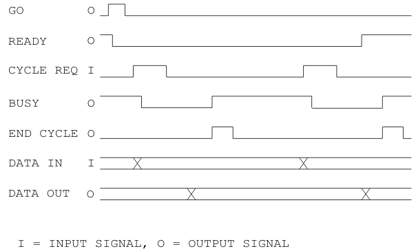
READY H Corresponds to the REDY bit in the Flags Register. When false it indicates that the DMA mechanism has been enabled and that the external device may issue cycle requests. READY H is set false by pulsing GO in the Pulse Command register, and is set true by MCLR or TERM in the Control or Pulse Command registers, by a bus initialize, by a true level on the ATTENTION input signal, or by range counter underflow. At end-of-range, READY H will go true either 50 or 100ns (switch option) prior to the trailing edge of the last BUSY H of the buffer. In buffer streaming mode, READY will remain false until the last word of the last buffer is being transferred.
BUSY H Indicates that the 10099 has received a valid cycle request, and is processing the input or output request. The trailing edge of BUSY H indicates that the request has been processed, and that the data from the device has been latched, or that data to the device is available. During DMA output, data to the device is stable either 50 or 100ns prior to the trailing edge of BUSY H.
The polarity of BUSY H is jumper-selectable on the 10099. Typically, BUSY H would be set to be high when asserted for so-called "device mode" applications, and asserted low for "interprocessor link mode" applications. In practice, most applications and devices will require that BUSY H is asserted low.
ACLO FNCT2 H This signal is set by writing a 1 to the FCN2 bit in the Control Register. It is pulsed for 270ns by writing a 1 to the FCN2 bit in the Pulse Command register. It is typically used to generate an ATTENTION H signal (and an interrupt) at the other DR11 in an interprocessor link.
GO H GO H is pulsed for 270ns when a 1 is written to the GO bit in the Control or Pulse Command registers. The leading edge of GO causes READY H to go false, and enables the 10099 to accept cycle requests from the attached device. GO may be used by the device to indicate that DMA is enabled, or it may be used as a strobe to indicate that the device should read the function lines, or the output data lines. (In some applications the initial value on the output data lines is used as a command, to be followed by DMA data in or out.)
END CYCLE H This is a 100ns pulse that begins simultaneously with the trailing edge of BUSY H. It may be used in place of the BUSY H trailing edge as a handshake signal. It should be noted that in a DEC DR11-W, END CYCLE H begins during busy and ends with the trailing edge of BUSY H, rather than beginning with the trailing edge of BUSY H as it does in IKON's DR11 emulators.
DI00-DI15 H Input data from the attached device. DI15 is the most significant bit. The state of these lines may be read by the program as the Data In Register, or may be transferred to memory during DMA input. During DMA input, these lines are latched either 50 or 100ns (switch option) after receiving a valid cycle request from the attached device.
PIXX H The IKON-specified optional input parity line. Odd parity is checked over 17 bits (DIxx and PIXX). Parity errors will set the PERR flag in the Status register, but will not halt or otherwise affect data transfers.
C0 CNTL H NOT SUPPORTED. The 10099 does not accept byte addressing or read-modify-write requests from the attached device. All external transfers are 16 bits wide.
C1 CNTL H This input may be used to control the direction of DMA transfers. If it is low, transfers will be from the 10099 to the attached device. If it is high, transfers will be from the attached device to the 10099. The C1 CNTL input must be stable by the trailing edge of the GO pulse in order to prepare the FIFOs for DMA transfer.
C1 CNTL may not be changed on a word-by-word basis as is possible with some DEC products.
There are two other options for DMA direction control available for use if the above condition cannot be met. A switch option allows using the FNCT1 output signal to control transfer direction. This is particularly useful for interprocessor links. The hardware link protocol uses FNCT1 for this purpose. Another switch option uses the SDIR bit in the Control register to replace the C1 CNTL input. In all cases, the selected input or bit must be stable by the trailing edge of the GO pulse. The polarities of the FNCT1 and SDIR bits are the same as the C1 CNTL input; low (0) for output and high (1) for input.
CYCLE RQ A,B H A 0-to-1 transition (edge) on either of these lines while the other is held low, or a simultaneous 0-to-1 transition on both inputs will request a DMA transfer to or from system memory. Such requests are honored only while READY H is false and BUSY H is not asserted. The 10099 will acknowledge the cycle request by asserting BUSY H. Once the input data has been captured, or the output data has been presented, BUSY H will be de-asserted, and the attached device may request another word transfer. Input data will be latched either 50 or 100ns after the active edge of a valid cycle request.
The polarity of the cycle request inputs is normally rising edge active. This may be changed to falling edge active by a jumper option on the 10099. Most applications will require cycle request polarity to be rising edge active.
A switch option allows holding CYCLE RQ B H at zero if for some reason it is not possible for the attached device to control CYCLE RQ B H.
ATTENTION H The ATTENTION H input signal can be used by the external device to terminate the DMA transfer (if DMA transfers are in progress) and/or interrupt the system's CPU. ATTENTION H sets READY H and the REDY bit in the Status register (they stay true if already set) and sets the ATTENTION flag (ATTF) in the Status register. If IENB (interrupt enable mask) is also true this will cause an interrupt request on the selected interrupt line.
If ATTENTION H is used to halt input data transfers, it should not be issued between the active edge of CYCLE RQx and the end of the associated BUSY H sequence, or that word of input data may not reach system memory.
For most applications - particularly interprocessor links - ATTENTION should be a pulse. If it is true when GO is pulsed, it will prevent the block transfer from starting. Transfers will not begin when ATTENTION is removed, and a new GO will have to be issued to commence transfers. The software controlling the 10099 should check to make sure that ATTENTION H has been de-asserted before attempting to start DMA transfers. ATTENTION H is driven by the other DR11's ACLO FNCT2 output in an interprocessor link configuration.
STATUS A,B,C H User defined input signals. These signals have no effect on the logic of the 10099, and may be read by the program as STTA, B, and C in the Status register.
WC INC ENB H NOT SUPPORTED. The 10099's FIFO-based logic does not allow external control of range counter incrementation.
BA INC ENB H NOT SUPPORTED. The 10099 does not allow external control of address counter incrementation.
A00 H NOT SUPPORTED. The 10099 does not allow byte wide DMA input operations.
BURST RQ L Not directly supported. The DEC DR11-W honors burst requests by "hogging" the bus for the duration of the block. During this time external handshaking (CYCLE RQ and BUSY) continues normally. The 10099 will support this type of transfer, but will not actually "hog" the bus. Other DR11-type products, such as the DRV11-B for the Q-bus do not handshake in burst mode, but do DMA accesses, and cycle BUSY H as fast as possible without waiting for cycle requests after the first one from the attached device. The 10099 does not support this type of transfer.
IMPORTANT NOTE: PLEASE READ THE FOLLOWING CABLE AND PIN-OUT DESCRIPTIONS
It is strongly recommended that IKON's ground-plane cables, or their equivalent, be used for connections between the Model 10099 and other devices. The DEC pin-out that we are required to emulate does not include alternate ground wires for each signal. As a result, data settling times and cross-talk become pattern sensitive. The only cable known to work well with this pin out is 40-conductor ground plane cable with a single drain wire connected to pin 40 (DEC's PIN A) at each end. This ground plane provides a stable impedance reference for all signals, and reduces settling times and cross-talk.
An example of a cable type suitable for this application is 3M 3476/40. A suitable insulation displacement connector compatible with the cable and the Model 10099's connectors is the 3M 3417 series.
The 10099 is capable of driving cables in excess of 100' long, providing that the cables are ground-plane type. The FAST/SLOW switch should be set according to cable length and the type of device to which the 10099 is connected. If the device at the other end of the cable samples data at the trailing edge of BUSY, or presents data at the leading edge of CYCLE REQUEST, the FAST setting is appropriate for cable lengths to 25', but is marginal at 50' (even ground-plane cable has some skew, and will cause slow signal edges when all data bits change at the same time). At 50', the SLOW setting should probably be used, unless the device adds some additional de-skew time to the output data and READY signal sampling point and/or additional settling time to the input data prior to issuing CYCLE REQUEST. An additional 50ns of de-skew/settling time is more than adequate for 50' cables when the FAST setting is used.
When the 10099 is connected to another 10099, or other DR11 or emulator, the FAST setting is acceptable for 50' cable lengths, as these devices have additional delays built in.
It is important to understand the pin-numbering convention used by the IKON family of DR11-W emulators, and how this convention relates to the DEC scheme.
The 10099's external connector pin-outs correspond electrically and mechanically with their DEC counterparts. DEC's connectors are numbered (lettered!) from A to VV, while IKON's connectors are numbered from 1 to 40 to remain consistent with IKON's other DR11 emulators. DEC's pin A corresponds to IKON's pin 40. The fact that DEC numbers their connector pins in reverse order when compared to the physical connectors available on the market has caused all kinds of grief to the customer trying to install DR11-W compatible products in a computer system. Some designers have chosen to make pin 1 correspond to DEC pin A, which produces a connector that is physically backward from the DEC product - and only adds to the confusion.
Customers using this or any other DR11-W compatible product must determine from their various suppliers which pin numbering convention is used, and whether the cables need a half-twist between connected devices.
Again, ground plane cable is best choice for data integrity. Ordinary ribbon cable does not give satisfactory performance unless it is very short - or the customer is very lucky! The drain wire in the ground plane cable is marked with a stripe and goes to IKON's pin 40, not pin 1 as with most computer cables.
IKON |
DEC |
SIGNAL |
DEC |
IKON |
|
1 |
VV |
DO15 H |
DO00 H |
UU |
2 |
3 |
TT |
DO14 H |
DO01 H |
SS |
4 |
5 |
RR |
DO13 H |
DO02 H |
PP |
6 |
7 |
NN |
DO12 H |
DO03 H |
MM |
8 |
9 |
LL |
DO11 H |
DO04 H |
KK |
10 |
11 |
JJ |
DO10 H |
DO05 H |
HH |
12 |
13 |
FF |
DO09 H |
DO06 H |
EE |
14 |
15 |
DD |
DO08 H |
DO07 H |
CC |
16 |
17 |
BB |
POXX H |
GROUND |
AA |
18 |
19 |
Z |
CYCLE RQ B H |
GROUND |
Y |
20 |
21 |
X |
END CYCLE H |
GROUND |
W |
22 |
23 |
V |
STATUS C H |
GROUND |
U |
24 |
25 |
T |
STATUS C H |
GROUND |
S |
26 |
27 |
R |
STATUS B H |
GROUND |
P |
28 |
29 |
N |
INIT H |
GROUND |
M |
30 |
31 |
L |
STATUS A H |
BURST RQ L |
K |
32 |
33 |
J |
WC INC ENB H |
GROUND |
H |
34 |
35 |
F |
READY H |
GROUND |
E |
36 |
37 |
D |
ACLO FNCT2 H |
GROUND |
C |
38 |
39 |
B |
CYCLE RQ A H |
GROUND |
A |
40 |
IKON |
DEC |
SIGNAL |
DEC |
IKON |
|
1 |
VV |
DI15 H |
DI00 H |
UU |
2 |
3 |
TT |
DI14 H |
DI01 H |
SS |
4 |
5 |
RR |
DI13 H |
DI02 H |
PP |
6 |
7 |
NN |
DI12 H |
DI03 H |
MM |
8 |
9 |
LL |
DI11 H |
DI04 H |
KK |
10 |
11 |
JJ |
DI10 H |
DI05 H |
HH |
12 |
13 |
FF |
DI09 H |
DI06 H |
EE |
14 |
15 |
DD |
DI08 H |
DI07 H |
CC |
16 |
17 |
BB |
PIXX H |
GROUND |
AA |
18 |
19 |
Z |
GROUND |
GROUND |
Y |
20 |
21 |
X |
GO H |
GROUND |
W |
22 |
23 |
V |
FNCT1 H |
GROUND |
U |
24 |
25 |
T |
C1 CNTL H |
GROUND |
S |
26 |
27 |
R |
FNCT2 H |
GROUND |
P |
28 |
29 |
N |
C0 CNTL H |
GROUND |
M |
30 |
31 |
L |
FNCT3 H |
FNCT3 H |
K |
32 |
33 |
J |
BA INC ENB H |
GROUND |
H |
34 |
35 |
F |
A00 H |
GROUND |
E |
36 |
37 |
D |
ATTENTION H |
GROUND |
C |
38 |
39 |
B |
BUSY H |
GROUND |
A |
40 |
P2-C |
Signal |
P2-A |
|
1 |
GROUND |
CYCLE RQ A |
1 |
2 |
GROUND |
ACLO FNGT2 |
2 |
3 |
GROUND |
READY |
3 |
4 |
WC INC ENB |
BURST RQ L |
4 |
5 |
STATUS A |
INIT |
5 |
6 |
STATUS B |
STATUS C |
6 |
7 |
STATUS C |
END CYCLE |
7 |
8 |
CYCLE RQ B |
POXX |
8 |
9 |
DO07 |
DO08 |
9 |
10 |
DO06 |
DO09 |
10 |
11 |
DO05 |
DO10 |
11 |
12 |
DO04 |
DO11 |
12 |
13 |
DO03 |
DO12 |
13 |
14 |
DO02 |
DO13 |
14 |
15 |
DO01 |
DO14 |
15 |
16 |
DO00 |
DO15 |
16 |
17 |
DI15 |
DI00 |
17 |
18 |
DI14 |
DI01 |
18 |
19 |
DI13 |
DI02 |
19 |
20 |
DI12 |
DI03 |
20 |
21 |
DI11 |
DI04 |
21 |
22 |
DI10 |
DI05 |
22 |
23 |
DI09 |
DI06 |
23 |
24 |
DI08 |
DI07 |
24 |
25 |
PIXX |
GROUND |
25 |
26 |
GO |
FNCT1 |
26 |
27 |
C1 CNTL |
FNCT2 |
27 |
28 |
CO CNTL |
FNCT3 |
28 |
29 |
FNCT3 |
BA INC ENB |
29 |
30 |
A00 |
GROUND |
30 |
31 |
ATTENTION |
GROUND |
31 |
32 |
BUSY |
GROUND |
32 |
The B row of the VMEbus P2 connector contains VMEbus signals.
The IKON Model 10099, like most DR11s and emulators, is capable of extensive self test under program direction. All Programmed-I/O, interrupt, and DMA features may be exercised and tested by "looping back" the J2 connector to the J1 connector. This is done with a 40-conductor ribbon cable connected pin-for-pin between two IDC sockets. It is also possible to perform loop-back via the P2 connector. This requires a 32 conductor cable that connects A1-16 to C32-17 and C1-16 to A32-17.
The signals connected in this way are shown below:
DO00-15 H > DI00-15 H
FNCT 1,2,3 H > STATUS C,B,A H
FNCT 1 H > C1 CNTL H
ACLO FNCT2 H > ATTENTION H
BUSY H > CYCLE RQ A H
POXX H > PIXX H
The loopback connection also causes (by virtue of the way the connector pin-outs line up) WC INC ENB H and BA INC ENB H to be asserted, and C0 CNTL H and CYCLE RQ B H to be held false. CYCLE RQ B H is the only one of these signals used by the 10099.
BUSY H should be jumpered for LOW assertion, and CYCLE REQUESTS should by jumpered to be RISING edge active. Link mode must be off for loop-back testing.
When set up for loopback, the 10099's features may be tested as follows:
Programmed-I/O is tested by writing a value to the Data Out Register, and verifying that the value appears in the Data In Register.
Function and Status bits are tested by writing the FCNx bits in the Control Register and reading the resulting STTx bits in the Status register. Note that FCN1 corresponds to STTC, and that setting FCN2 will cause the ATTN, and ATTF bits to set. Clearing FCN2 will clear the ATTN bit, but should leave the ATTF bit set.
Interrupts and various pulse commands are tested by setting the board's interrupt mask, and then generating an ATTENTION interrupt by pulsing ACLO FNCT2 by writing a 1 to the FCN2 bit in the Pulse Command register. DMA interrupt conditions may be tested during DMA testing.
DMA output is tested by setting the 10099's Range, Address, and Address Modifier registers to appropriate values, setting FCN1 or SDIR to 0, and then Pulsing GO and CYCLE in the Pulse Command register. GO clears the REDY bit and allows the 10099 to accept cycle requests and perform DMA transfers and CYCL actually initiates the first transfer. The end of the first, and later transfers cause BUSY H to go from low to high, which causes another cycle request, continuing the handshake until the Range Count has been exhausted. End-of-range sets the REDY bit and the DMAF bit in the Status register.
If the data buffer has been previously set to a known pattern, the last word of that pattern should appear in the Data In Register when the DMA block transfer is complete.
DMA input is tested in the same way except that the system's DMA logic is set up for input and the 10099's SDIR or FCN1 bit is set to 1 prior to starting transfers. If a known value has been previously written to the Data Out Register, that value should be repeated in every word of the input buffer in memory.
The IKON Model 10099 may be used in a very high-speed parallel interprocessor link with other IKON DR11-W emulators, or those made by DEC or other manufacturers. This technique of linking processors and systems produces high transfer rates, and can usually be implemented with a simple, efficient protocol.
The physical interprocessor link connection is made by connecting the J1 connector of each DR11-W to the J2 connector of the other DR11-W, and setting up each board for BUSY H asserted low and CYCLE REQ rising edge active. Two 10099s may also be linked by connecting a 64 conductor ground plane cable between the P2 connectors of each board. The cable should have a half twist - either by actually fabricating a cable with a twist, or by simply plugging in one connector upside down.
The signal connection accomplished by pin-for-pin cables between the DR11s is similar to loop-back, and is shown below.
DR11-W #1 DR11-W #2
DO00-15 H > DI00-15 H
POXX H > PIXX H
DI00-15 H < DO00-15 H
PIXX H < POXX H
BUSY H > CYCLE RQ A H
CYCLE RQ A H < BUSY H
FNCT 1,2,3 H > STATUS C,B,A H
STATUS C,B,A H < FNCT 1,2,3 H
FNCT1 H > (loop back
C1 CNTL H < to #1)
(loop back < FNCT1 H
to #2) > C1 CNTL H
FNCT3 H > BURST RQ L
BURST RQ L < FNCT3 H
ACLO FNCT2 H > ATTENTION H
ATTENTION H < ACLO FNCT2 H
CYCLE RQ B H < 0
C0 CNTL H < 0
A00 H < 0
WC INC ENB H < 1
BA INC ENB H < 1
0 > CYCLE RQ B H
0 > C0 CNTL H
0 > A00 H
1 > WC INC ENB H
1 > BA INC ENB H
Note that each device's C1 CNTL H (direction control) is derived from its own FNCT1 H output. If the device sets its FNCT1 H output to 1, it will be doing an input into its associated memory.
The exact interprocessor link protocol chosen is customer and application dependent, but most are based on the link protocol suggested by DEC in its DR11-W user's guide. This protocol involves exchanging single word messages via ATTENTION H interrupts to set up word count and data direction, and synchronize the start of DMA transfers. Block mode DMA accomplishes the actual data transfer. An example of an enhanced version of this protocol is available on request.
When ATTENTION H is used as part of a DMA protocol (typically driven by ACLO FNCT2 H as a clear-to-send indicator), it must be a pulse rather than a level. If the program that received the ATTENTION H is signal attempts to start DMA by pulsing GO while ATTENTION H is still asserted, DMA operation will be inhibited, and will not start when the ATTENTION H signal is de-asserted. The end of the link generating the ATTENTION H signal should use a pulse that is as short as possible - which may be relatively long if more that one operating system call is required - and the end of the link receiving the ATTENTION H signal should wait until it is removed before pulsing GO.
The IKON Model 10099 Pulse Command register may be used to generate a 270ns ACLO FNCT2 pulse to pulse ATTENTION at the other DR11.
NOTE: In an interprocessor link, each DR11s BURST RQ L input is driven by the other end's FNCT3 H output. FNCT3 H should be set to 1 at each end of the link during DMA data transfers to prevent burst DMA requests. DR11 burst-style transfers are not allowed in interprocessor link applications, and may cause adverse effects on devices on the other system's bus and/or cause the handshaking between DR11s to break down. This is not a problem with IKON's emulators, but may be with DEC's and other manufacturers. As a matter of style, it is a good idea to set FCN3 during DMA transfers with any DR11-type link.
When two IKON DR11 emulators are linked, the "I-link" mode may be selected via switches to give improved performance. This is done by shortening certain timing parameters. If two IKON Model 10099 DR11 emulators are linked, the "U-link" mode may be selected, which can give much higher performance than normal DR11 links. This is accomplished by using "semi-synchronous" handshaking on the cable, which only requires a handshake from the receiving 10099 every 128 words. This effectively cuts the handshake time in half (by not waiting for a handshake from the receiver) and eliminates the effect of cable delays on the handshake.
The IKON 10099 has switch and jumper options that allow accommodating many system configurations and applications. The options controlled by jumpers and switches are listed on the following pages.
jumper pins effect
connected
E2-1 to E2-2 BUSY asserted low
E2-2 to E2-3 BUSY asserted high
E1-1 to E1-2 CYCLE REQUESTS rising edge active
E1-2 to E1-3 CYCLE REQUESTS falling edge active
E3-2 to E3-3 16 bit range counter
E3-1 to E3-2 24 bit range counter
E4-1 to E4-2 Enable CYCLE REQ B
E4-2 to E4-3 Ground CYCLE REQ B
E5 bus grant level
E6 bus request level
E8 interrupt request level
E7 interrupt ack level
U49 |
address bit |
U50 |
address bit |
U51 |
add bit/ function |
U52 |
function |
1 |
A23 |
1 |
A15 |
1 |
A07 |
1 |
dir=FCN1 |
2 |
A22 |
2 |
A14 |
2 |
A06 |
2 |
dir=C1CNTL |
3 |
A21 |
3 |
A13 |
3 |
A05 |
3 |
dir=SDIR |
4 |
A20 |
4 |
A12 |
4 |
16 bit map |
4 |
D32 enable |
5 |
A19 |
5 |
A11 |
5 |
DFLG = 1 |
5 |
sel FAST |
6 |
A18 |
6 |
A10 |
6 |
PERR enable |
6 |
*sel LINK |
7 |
A17 |
7 |
A09 |
7 |
swap P-I/O |
7 |
block sel 1 |
8 |
A16 |
8 |
A08 |
8 |
swap DMA |
8 |
block sel 0 |
* IKON links only
The location of the 10099's on-board register set in the system memory map(s) is determined by switches at U49, U50, and U51. (Some switches at U51 are also used for other functions.)
Each switch labelled with an Axx determines whether a 1 or a 0 will be decoded in that address bit position. Note that the address switches are complemented. A switch set to ON will decode a 0 in that bit position.
Address map selection is done with switch U51-4. If that switch is OFF, the board will respond to any of the four standard map address modifier codes: (hex) 39, 3A, 3D, and 3E, and will decode 24 address bits. If U51-4 is ON, the board will respond to either of the short I/O map address modifier codes: 29 and 2D, and will decode only the low 16 bits of the address bus.
In order for the 10099 to recognize its address, it must see its selected address pattern on the VMEbus address bits, and the selected address modifier code on the VMEbus address modifier bits.
To set up the board to decode address (hex) D00000 in the 24 bit (standard) memory map, the 10099's switches would be set as follows:
U49 |
address bit |
U50 |
address bit |
U51 |
add bit/ function |
1 |
OFF |
1 |
ON |
1 |
ON |
2 |
OFF |
2 |
ON |
2 |
ON |
3 |
ON |
3 |
ON |
3 |
ON |
4 |
OFF |
4 |
ON |
4 |
OFF |
5 |
ON |
5 |
ON |
5 |
xxx |
6 |
ON |
6 |
ON |
6 |
xxx |
7 |
ON |
7 |
ON |
7 |
xxx |
8 |
ON |
8 |
ON |
8 |
xxx |
DFLG is a "do-nothing" bit in the LSB of the Status register. It may be used for any purpose - such as indicating to the software that the board is a 10099 rather than a 10084 - which always has a 0 as the LSB of its status register, or a 10089, which has a selectable DFLG. The 10084 and 10089 are IKON's other VMEbus DR11-W emulators.
If switch U51-5 is on, DFLG will be read as a 1. If it is off, DFLG will be read as a 0
The bus interrupt level of the board is controlled by jumpers E7, and E8. The jumpers for RQ and ACK must be set to the same level.
E8 INT RQ E7 INT ACK
13-14 IR1 13-14 IA1
11-12 IR2 11-12 IA2
9-10 IR3 9-10 IA3
7-8 IR4 7-8 IA4
5-6 IR5 5-6 IA5
3-4 IR6 3-4 IA6
1-2 IR7 1-2 IA7
To select bus interrupt level 4 connect E7-7 to E7-8, and E8-7 to E8-8.
Bus interrupt level is often referred to as "priority" by system and CPU manufacturers.
The bus priority level used by the board when it is a bus master (during DMA transfers) is selected by jumpers E5 and E6. The bus request and grant levels selected must agree!
Bus Request Selection
E6 Bus Level
1-2 BR0
3-4 BR1
5-6 BR2
7-8 BR3
Bus Grant Matrix
Bus Grant E5 Internal Grant
BG0IN 1 2 BGIN
BG0OUT 3 4 BGOUT
BG1IN 5 6 BGIN
BG1OUT 7 8 BGOUT
BG2IN 9 10 BGIN
BG2OUT 11 12 BGOUT
BG3IN 13 14 BGIN
BG3OUT 15 16 BGOUT
The bus level to be used by the 10099 is selected by jumpering the appropriate BGxIN pin to the adjacent BGIN pin, and the corresponding BGxOUT pin to the adjacent BGOUT pin. The three remaining bus levels are passed through the board by jumpering each level's BGxIN pin to its BGxOUT pin. The BRQx jumpers must also be set to the matching level.
A board set up to use bus level 3 would have the following jumpers in place:
E6-7 to 8, E5-1 to 3, 5 to 7, 9 to 11, 13 to 14, and 15 to 16
Consult target system documentation for information on selecting the correct bus priority level for this board. Some systems support all four bus levels. Some only support a single level, which, by VMEbus specification, is level 3.
The number of words or longwords per bus arbitration that are transferred to or from the FIFOs is set by switches U52-7 and 8. Whether words or longwords are transferred is determined by the 32 bit enable switch and the software.
U52 switch 7 8
4 xfers OFF OFF
16 xfers OFF ON
64 xfers ON OFF
256 xfers ON ON
The block length referred to here applies only to traffic on the VMEbus - not to communications with the attached device. The attached device is "uncoupled" from these bursts by the input and output FIFOs. This type of blocking is not the same as the burst transfers available with some DR11-type products which allow the device to force the DR11 to "hog" the bus. The 10099 does not support this type of burst transfer and does not allow the external device to control block size.
The 10099 is capable of transferring data to and from VMEbus accessible memory 32 bits at a time. If switch U52-4 is OFF, data width on the bus will be 16 bits. If switch U52-4 is ON, data width will be 32 bits, which will double the 10099's bus efficiency. If this option is to be used, the VMEbus memory involved must be capable of honoring 32 bit (longword) data requests. In either 16 or 32 bit DMA data mode, the path to the external device remains 16 bits wide. The data width used on the bus is transparent to the device and the software.
In 32-bit mode, the first and/or last transfers of a buffer may be 16 bits only, depending on odd/even address and range values.
The software may override 32 bit data width selection by setting the FD16 bit in the address modifier register. This will force the 10099 to do all transfers in 16 bit mode.
IKON's 10089 and 10093 VMEbus DR11-W and DR11-WX emulators included a jumper option that controlled when the output FIFOs began to read data from the VMEbus. The 10099 does not include this option. Its output FIFOs will not start to read data from the VMEbus until the first CYCLE REQUEST or CYCL command has been received. Some devices use the GO pulse to indicate a non-DMA command, in addition to a DMA enable function. The 10099's FIFO load hold-off feature prevents FIFO loading and the associated DMA bus traffic in the cases when GO is used as a non-DMA command.
If jumper pins E3-2 and 3 are connected, the range counter will be 16 bits long. This allows a maximum count of 64K words. If jumper pins E3-1 and 2 are connected, the range counter will be 24 bits long, giving a maximum count of 16M words. If the range counter length is set to 24 bits, all 24 bits must be set to the appropriate values before starting DMA. The 16 bit mode is included to retain software compatibility with IKON's other DR11 emulators.
Switches at U51 control the byte ordering of the data to and from the external device. U51-8 controls DMA byte ordering, and U51-7 controls P-I/O byte ordering.
U51 switch 7 8
swap DMA data X ON
no DMA swap X OFF
swap P-I/O bytes ON X
no P-I/O swap OFF X
This hardware option is an IKON extension of the Digital Equipment Corporation DR11-W specification. It replaces two ground pins with parity in and out signal pairs. The 10099 provides parity checking on all data transfers over the DR11 cables. Odd parity is maintained and checked over 17 bits (16 data bits + 1 parity bit). This parity checking applies only to P-I/O and DMA data transferred over the external cables, and not to traffic on the VMEbus. The attached device, or other DR11-W type interface must have matching parity logic for this enhancement to be used.
Outgoing parity is generated and latched whenever the data is written to the Output Data register by P-I/O or DMA. After power-up parity on the output lines may not be correct until this register has been written by the software or a DMA output has been done. Incoming parity is checked during P-I/O and DMA reads of the Input Data register. Any read parity error causes the PERR flag in the Status register to set, and remain set until cleared by MCLR or RPER. PERR is a status bit only; its setting does not halt transfers or generate an interrupt. It is intended that this bit be checked after a DMA block or P-I/O word transfer is complete.
Switch U51-6 controls whether parity errors are reported in the status register. If U51-6 is ON, external parity errors will be reported in the PERR bit in the Status register. If U51-6 is OFF, errors will not be reported, and PERR will always be 0.
The jumper pins at E2 control the polarity of the outgoing BUSY signal.
If jumper pins E2-1 and 2 are connected, BUSY will be asserted LOW, which is used for interprocessor links, and most other applications. If pins E2-2 and 3 are connected, BUSY will be asserted high.
Jumper pins at E1 determine the active edge of the incoming CYCLE REQ A and B signals.
If jumper pins E1-1 and 2 are connected, cycle requests will be rising edge active. If jumper pins E1-2 and 3 are connected, cycle requests will be falling edge active.
Rising edge active is normal for all known DR11 applications.
Jumper E4 may be used to inhibit the CYCLE REQ B input. This may be useful in situations when the attached device does not control the CYCLE RQ B input.
Connecting E4-1 to 2 enables CYCLE RQ B. Connecting E4-2 to 3 GROUNDS this input.
Unlike the Digital Equipment Corporation's DR11-W, and some other emulators, the 10099 requires that the direction of transfer be known by the DMA logic prior to the trailing edge of the GO pulse. This is necessary for proper FIFO operation. Normally, the transfer direction is determined by the incoming C1 CNTL signal. If it is not possible for the external device to guarantee that this input will be stable prior to the end of GO, there are two other options which may be used to determine transfer direction; direction may be controlled by the FCN1 bit in the Control register, or by the SDIR (software direction) bit in the Control register.
Switches U52-1, 2, and 3 control the source of direction control.
U52 switch 1 2 3
FCN1 ON OFF OFF
C1 CNTL OFF ON OFF
SDIR OFF OFF ON
Input De-Skew & Output Settling Times
Input de-skew (CYCLE RQ to input data latched) and output settling time (data stable to BUSY trailing edge), and READY assertion to BUSY trailing edge (during the last word of the buffer) are controlled by switch U52-5.
If U52-5 is ON, all the above timings will be 50ns. If it is OFF, they will be 100ns. The 50ns timing should be used whenever device and cable quality allow. The FAST setting is acceptable for cable lengths to 25'. SLOW mode should be used for 50' cables unless the attached device includes some delay after the trailing edge of BUSY before the output data lines and READY or sampled and/or some additional settling time to the input data before CYCLE RQ is issued.
An additional settling/de-skew delay of 50ns is sufficient to allow the FAST setting to be used with 50ns cables.
When the 10099 is connected to another DR11 or emulator, the FAST setting may be used for all cable lengths, as these devices typically include some de-skew and setting time at their end.
When two IKON DR11 emulators are linked together, it is possible to increase performance by selecting link mode timing. One timing mode is used when a 10099 is linked to another IKON product ( which is not a '99). Another, much higher performance mode is available when two 10099s are linked. These modes are to be used only between IKON products. When linking to other DR11-type devices. U52-6 (Link) should be off, and U52-7 (Fast/Slow) set according to the other device's timing requirements.
When a 10099 is linked to another IKON emulator, it is possible to shorten the input and output de-skew and setup times while still preserving data integrity. ("I-link" mode.) This is possible because the minimum handshake times are known for both ends of the link, and each end can "cheat" on its BUSY timing without risking having the other end issue a new CYCLE REQ too soon.
When two 10099s are linked a special "semi-synchronous" handshake is used. ("U-link" mode.) It eliminates the handshake delay at the receiving end of the link, and the handshake delay due to cable length. Sustained transfer rates of 8Mbytes/second may be achieved in this mode.
Turning on switch U52-6 (Link) selects IKON link timing.
U52-5 (Fast/Slow) should be OFF (Slow) for IKON to IKON links, and ON (Fast) for 10099 to 10099 links.
NOTE: Boards prior to Revision A do not provide for "U-link" mode. They are set up for "I-link" operation by turning ON both the Link and Fast switches.
Note on BUSY and END CYCLE Timing
It should be noted that the IKON DR11-W emulator differs from the Digital Equipment Corporation (DEC) product in one respect (other than being much faster!); in the DEC product, the trailing edge of END CYCLE is co-incident with the trailing edge of BUSY. In the 10099, and other IKON DR11 emulators, the leading edge of END CYCLE is co-incident with the trailing edge of BUSY. This should not prove to be a problem, as all known applications use either BUSY or END CYCLE, but not both. Further, DEC's Q-bus products do not support END CYCLE at all. New applications should use BUSY rather than END CYCLE to ensure compatibility with future DR11-type products.
See Detailed Specifications and Hardware Options sections for exact timings.